
Datasheet


f =
-3dB
ln(2)(n + 1)
2 tp
ACQ
R <
SOURCE
t
ACQ
C ln(2)(n + 1)
S
- (R + R )
SER SW
ADS8363
ADS7263
ADS7223
www.ti.com
SBAS523B –OCTOBER 2010–REVISED JANUARY 2011
Acquisition is indicated with the BUSY signal being It is important to keep the voltage to all inputs within
low. It starts by closing the input switches (after the 0.3V limit below AGND and above AVDD, while
finishing the previous conversion and precharging) not allowing dc current to flow through the inputs
and finishes with the rising edge of the CONVST (exceeding these limits causes the internal ESD
signal. If the device operates at full speed, the diodes to conduct, leading to increased leakage
acquisition time is typically 100ns. current that may damage the device). Current is only
necessary to recharge the sample-and-hold
The minimum –3dB bandwidth of the driving
capacitors.
operational amplifier can be calculated as shown in
Equation 1, with n = 16 for the resolution of the Unused inputs should be directly tied to AGND or
ADS8363, n = 14 for the ADS7263, or n = 12 for the RGND without the need of a pull-down resistor.
ADS7223:
Analog-to-Digital Converters (ADCs)
The ADS8363/7263/7223 include two SAR-type,
(1)
1MSPS, 16-/14-/12-bit ADCs that include
With t
ACQ
= 100ns, the minimum bandwidth of the sample-and-hold (S&H), respectively, as shown in the
driving amplifier is 19MHz for the ADS8363, 17MHz Functional Block Diagram on the front page of this
for the ADS7263, and 15MHz for the ADS7223. The data sheet.
required bandwidth can be lower if the application
allows a longer acquisition time. CONVST
A gain error occurs if a given application does not The analog inputs are held with the rising edge of the
fulfill the settling requirement shown in Equation 1. CONVST (conversion start) signal. The setup time of
However, linearity and THD are not directly affected CONVST referred to the next rising edge of CLOCK
as a result of precharging the capacitors. (system clock) is 12ns (minimum). The conversion
automatically starts with the rising CLOCK edge. A
The OPA365 from Texas Instruments is
rising edge of CONVST should not be issued during a
recommended as a driver; in addition to offering the
conversion (that is, when BUSY is high).
required bandwidth, it also provides a low offset and
excellent THD performance (see also Application RD (read data) and CONVST can be shorted to
Information section). minimize necessary software and wiring. The RD
signal is triggered by the device on the falling edge of
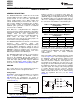
The phase margin of the driving operational amplifier
CLOCK. Therefore, the combined signals must be
is usually reduced by the ADC sampling capacitor. A
activated with the rising CLOCK edge. The
resistor placed between the capacitor and the
conversion then starts with the subsequent rising
amplifier limits this effect; therefore, an internal 100Ω
CLOCK edge. In modes with only SDOA active (that
resistor (R
SER
) is placed in series with the switch. The
is, in modes II, IV, SII, and SIV), the maximum length
switch resistance (R
SW
) is typically 100Ω, as shown in
of the combined RD and CONVST signal is one clock
Figure 28).
cycle if the half-clock timing is used.
An input driver may not be required, if the impedance
If CONVST and RD are combined, CS must be low
of the signal source (R
SOURCE
) fulfills the requirement
whenever a new conversion starts; however, this
of Equation 2:
condition is not required if RD and CONVST are
controlled separately. Note that if FIFO is used,
CONVST must be controlled separately from RD.
After completing a conversion, the sample capacitors
Where:
are automatically precharged to the value of the
n = 16/14/12 for the resolution of the
reference voltage used to significantly reduce the
ADS8363/7263/7223, respectively.
crosstalk among the multiplexed input channels.
C
S
= 40pF sample capacitance.
CLOCK
R
SER
= 100Ω input resistor value.
R
SW
= 100Ω switch resistance value. (2)
The ADS8363/7263/7223 use an external clock with
an allowable frequency range that depends on the
With t
ACQ
= 100ns, the maximum source impedance
mode being used. By default (after power-up), the
should be less than 12Ω for the ADS8363, less than
ADC operates in half-clock mode, which supports a
40Ω for the ADS7263, and less than 77Ω for the
clock in the range of 0.5MHz to 20MHz. In full-clock
ADS7223. The source impedance can be higher if the
mode, the ADC requires a clock in the range of 1MHz
ADC is used at a lower data rate.
to 40MHz. For maximum data throughput, the clock
The differential input voltage range of the ADC is
±V
REF
, the voltage at the selected REFIOx pin.
Copyright © 2010–2011, Texas Instruments Incorporated Submit Documentation Feedback 17
Product Folder Link(s): ADS8363 ADS7263 ADS7223