
Datasheet


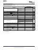


TIMING CHARACTERISTICS
(1) (2)
: 1.8V
ADS7229
ADS7230
www.ti.com
............................................................................................................................................................... SBAS437A – MAY 2008 – REVISED JUNE 2009
All specifications typical at – 40 ° C to 85 ° C, +VA = 2.7 V, and +VBD = 1.8V, unless otherwise noted.
ADS7229, ADS7230
PARAMETER MIN TYP MAX UNIT
External, 3V ≤ +VA ≤ 3.6V,
0.5 21
f
CCLK
= 1/2 f
SCLK
External, 2.7V ≤ +VA ≤ 3V,
f
CCLK
Frequency, conversion clock, CCLK 0.5 18.9 MHz
f
CCLK
= 1/2 f
SCLK
Internal,
20 22.3 23.5
f
CCLK
= 1/2 f
SCLK
t
1
Setup time, falling edge of CS to EOC 1 CCLK
t
2
Hold time, falling edge of CS to EOC 0 ns
t
CL
Pulse duration, CONVST low 40 ns
t
3
Hold time, falling edge of CS to EOS 20 ns
t
4
Setup time, rising edge of CS to EOS 20 ns
t
5
Hold time, rising edge of CS to EOS 20 ns
Setup time, falling edge of CS to first t
6
falling
t
6
5 ns
SCLK
t
SCLKL
Pulse duration, SCLK low 8 t
SCLK
– 8 ns
t
SCLKH
Pulse duration, SCLK high 8 t
SCLK
– 8 ns
All modes,
23.8 2000
3V ≤ +VA ≤ 3.6V
t
SCLK
Cycle time, SCLK ns
All modes,
26.5 2000
2.7V ≤ +VA < 3V
t
H2
Hold time, falling edge of SCLK to SDO invalid 10pF load 7.5 ns
t
D1
Delay time, falling edge of SCLK to SDO valid 10pF load 16 ns
10pF load,
13
2.7V ≤ +VA ≤ 3V
Delay time, falling edge of CS to SDO valid,
t
D2
ns
SDO MSB output
10pF load,
11
3V ≤ +VA ≤ 3.6V
t
S1
Setup time, SDI to falling edge of SCLK 8 ns
t
H1
Hold time, SDI to falling edge of SCLK 4 ns
Delay time, rising edge of CS/FS to SDO
t
D3
8 ns
3-state
Setup time, 16th falling edge of SCLK t
7
t
7
10 ns
before rising edge of CS/FS
(1) All input signals are specified with t
r
= t
f
= 1.5ns (10% to 90% of VBD) and timed from a voltage level of (V
IL
+ V
IH
)/2.
(2) See timing diagrams.
Copyright © 2008 – 2009, Texas Instruments Incorporated Submit Documentation Feedback 9
Product Folder Link(s): ADS7229 ADS7230