
Datasheet


www.ti.com
TIMING CHARACTERISTICS
(1) (2)
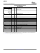
Input Clock
Analog
Input
Signal
Sample
N
N + 1
N + 2
N + 3
N + 4
N + 14
N + 16
N + 17
N + 15
N − 17 N − 16 N − 15 N − 14 N − 13 N − 3 N − 2 N − 1 N
t
su
t
h
t
START
t
A
t
END
t
PDI
Data Out
(D0−D11)
17.5 Clock Cycles
Data Invalid
Output Clock
ADS5542
SBAS308D – MAY 2004 – REVISED FEBRUARY 2007
Typical values given at T
A
= 25 ° C, min and max specified over the full recommended operating temperature range, AV
DD
=
DRV
DD
= 3.3 V, sampling rate = 80 MSPS, 50% clock duty cycle, 3-V
PP
differential clock, and C
LOAD
= 10 pF, unless
otherwise noted
PARAMETER DESCRIPTION MIN TYP MAX UNIT
Switching Specification
t
A
Aperture delay Input CLK falling edge to data sampling point 1 ns
Aperture jitter (uncertainty) Uncertainty in sampling instant 300 fs
t
SETUP
Data setup time Data valid
(3)
to 50% of CLKOUT rising edge 3.2 4.2 ns
t
HOLD
Data hold time 50% of CLKOUT rising edge to data becoming invalid
(3)
1.8 3.0 ns
t
START
Input clock to output data valid Input clock rising edge to data valid start delay 3.8 5.0 ns
start
(4) (5)
t
END
Input clock to output data valid Input clock rising edge to data valid end delay
(4) (5)
8.4 11.0 ns
end
t
JIT
Output clock jitter Uncertainty in CLKOUT rising edge, peak-to-peak 210 315 ps
PP
t
r
Output clock rise time Rise time of CLKOUT from 20% to 80% of DRV
DD
2.5 2.8 ns
t
f
Output clock fall time Fall time of CLKOUT from 80% to 20% of DRV
DD
2.1 2.3 ns
t
PDI
Input clock to output clock Input clock rising edge, zero crossing, to output clock rising 7.1 8.0 8.9 ns
delay edge 50%
t
r
Data rise time Data rise time measured from 20% to 80% of DRV
DD
5.8 6.6 ns
t
f
Data fall time Data fall time measured from 80% to 20% of DRV
DD
4.4 5.3 ns
Output enable(OE) to data Time required for outputs to have stable timings with regard to 1000 Clock
output delay input clock
(6)
after OE is activated cycles
Time to valid data after coming out of software power down 1000
Clock
Wakeup time
cycles
Time to valid data after stopping and restarting the clock 1000
Latency Time for a sample to propagate to the ADC outputs 17.5 Clock
cycles
(1) Timing parameters are ensured by design and characterization, and not tested in production.
(2) See Table 5 through Table 6 in the Application Information section for timing information at additional sampling frequencies.
(3) Data valid refers to 2 V for LOGIC HIGH and 0.8 V for LOGIC LOW.
(4) See the Output Information section for details on using the input clock for data capture.
(5) These specifications apply when the CLKOUT polarity is set to rising edge (according to Table 2 ). Add 1/2 clock period for the valid
number for a falling edge CLKOUT polarity.
(6) Data outputs are available within a clock from assertion of OE; however, it takes 1000 clock cycles to ensure stable timing with respect
to input clock.
A. It is recommended that the loading at CLKOUT and all data lines are accurately matched to ensure that the above
timing matches closely with the specified values.
Figure 1. Timing Diagram
6
Submit Documentation Feedback