
Datasheet


14-Bit
ADC
14b
DigitalFunctions
(Gain,OffsetCorrection,TestPatterns)
Output
Interface
DDRLVDS
orCMOS
14b
DISLOWLATENCYPin
ADS4126
,
ADS4129
ADS4146
,
ADS4149
www.ti.com
SBAS483G – NOVEMBER 2009–REVISED JANUARY 2011
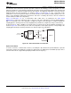
DIGITAL FUNCTIONS AND LOW LATENCY MODE
The device has several useful digital functions such as test patterns, gain, and offset correction. All of these
functions require extra clock cycles for operation and increase the overall latency and power of the device.
Alternately, the device has a low-latency mode in which the raw ADC output is routed to the output data pins with
a latency of 10 clock cycles. In this mode, the digital functions are bypassed. Figure 122 shows more details of
the processing after the ADC.
The device is in low-latency mode after reset. In order to use any of the digital functions, first the low-latency
mode must be disabled by setting the DIS LOW LATENCY register bit to '1'. After this, the respective register bits
must be programmed as described in the following sections and in the Serial Register Map section.
Figure 122. Digital Processing Block Diagram
GAIN FOR SFDR/SNR TRADE-OFF
The ADS412x/4x include gain settings that can be used to get improved SFDR performance. The gain is
programmable from 0dB to 6dB (in 0.5dB steps) using the GAIN register bits. For each gain setting, the analog
input full-scale range scales proportionally, as shown in Table 11.
The SFDR improvement is achieved at the expense of SNR; for each gain setting, the SNR degrades
approximately between 0.5dB and 1dB. The SNR degradation is reduced at high input frequencies. As a result,
the gain is very useful at high input frequencies because the SFDR improvement is significant with marginal
degradation in SNR. Therefore, the gain can be used to trade-off between SFDR and SNR.
After a reset, the device is in low-latency mode and gain function is disabled. To use gain:
• First, disable the low-latency mode (DIS LOW LATENCY = 1).
• This setting enables the gain and puts the device in a 0dB gain mode.
• For other gain settings, program the GAIN bits.
Table 11. Full-Scale Range Across Gains
GAIN (dB) TYPE FULL-SCALE (V
PP
)
0 Default after reset 2
1 Programmable gain 1.78
2 Programmable gain 1.59
3 Programmable gain 1.42
4 Programmable gain 1.26
5 Programmable gain 1.12
6 Programmable gain 1.00
Copyright © 2009–2011, Texas Instruments Incorporated Submit Documentation Feedback 63
Product Folder Link(s): ADS4126 ADS4129 ADS4146 ADS4149