
Datasheet


0 0.5 1 1.5 2 2.5 3 3.5 4
68
71
74
77
80
83
86
89
92
60
62
64
66
68
70
72
74
76
Differential Clock Amplitude (V
PP
)
SFDR (dBc)
SNR (dBFS)
SFDR
SNR
Input Frequency = 150MHz
66
67
68
69
70
71
72
73
74
75
30 35 40 45 50 55 60 65 70
Input Clock Duty Cycle (%)
SNR (dBFS)
Default
Low−Speed Mode Enabled
Input Frequency = 10MHz
−1.5
−1
−0.5
0
0.5
1
1.5
0 2048 4096 6144 8192 10240 12288 14336 16384
Output Code (LSB)
INL (LSB)
0
OutputCode(LSB)
8170 8179
CodeOccurrence(%)
8171 8172 8175 8177
35
10
15
20
25
30
5
8173 8174 8176 8178
ADS4122, ADS4125
ADS4142, ADS4145
www.ti.com
SBAS520A –FEBRUARY 2011– REVISED MARCH 2011
TYPICAL CHARACTERISTICS: ADS4145 (continued)
At +25°C, AVDD = 1.8V, DRVDD = 1.8V, maximum rated sampling frequency, sine wave input clock, 1.5V
PP
differential clock
amplitude, 50% clock duty cycle, –1dBFS differential analog input, 0dB gain, low-latency mode, DDR LVDS output interface,
and 32k-point FFT, unless otherwise noted.
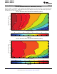
PERFORMANCE ACROSS INPUT CLOCK AMPLITUDE SNR ACROSS INPUT CLOCK DUTY CYCLE
Figure 87. Figure 88.
OUTPUT NOISE HISTOGRAM
INTEGRAL NONLINEARITY (with Inputs Shorted to VCM)
Figure 89. Figure 90.
Copyright © 2011, Texas Instruments Incorporated Submit Documentation Feedback 53
Product Folder Link(s): ADS4122 ADS4125 ADS4142 ADS4145