
Datasheet


CLK
SYNC
t
SSC
t
HSC
FSO
t
C
t
SYPW
t
STL
CLK
FSO
t
CPW
SCLK
t
CS
t
CF
t
FPW
DOUT
t
DS
t
DH
MSB
BIT
14
LSB
NewData
BIT
1
t
CPW
ADS1602
SBAS341E –DECEMBER 2004–REVISED OCTOBER 2011
www.ti.com
TIMING DIAGRAMS
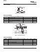
Figure 1. Initialization Timing
TIMING REQUIREMENTS
For T
A
= –40°C to +85°C, DVDD = 2.7V to 3.6V, and IOVDD = 2.7V to 5.25V.
SYMBOL DESCRIPTION MIN TYP MAX UNIT
t
SYPW
SYNC positive pulse width 1 CLK period
t
C
Clock period (CLK) 25 ns
t
SSC
Setup time; SYNC rising edge to CLK rising edge 0.5 CLK period
t
HSC
Hold time; CLK rising edge to SYNC falling edge 0.5 CLK period
Settling time of the ADS1602; FSO falling edge to next
t
STL
833 CLK periods
FSO rising edge
Figure 2. Data Retrieval Timing
TIMING REQUIREMENTS
For T
A
= –40°C to +85°C, DVDD = 2.7V to 3.6V, and IOVDD = 2.7V to 5.25V.
SYMBOL DESCRIPTION MIN TYP MAX UNIT
t
CS
Rising edge of CLK to rising edge of SCLK 15 ns
t
CF
Rising edge of SCLK to rising edge of FSO 5 ns
t
CPW
CLK positive or negative pulse width 11.25 ns
t
FPW
Frame sync output high pulse width 1 CLK period
t
DS
SCLK rising edge to new DOUT valid 5 ns
t
DH
SCLK falling edge to DOUT invalid 6 ns
8 Copyright © 2004–2011, Texas Instruments Incorporated