
Datasheet


ADS1294, ADS1294R
ADS1296, ADS1296R
ADS1298, ADS1298R
www.ti.com
SBAS459I –JANUARY 2010–REVISED JANUARY 2012
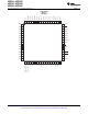
PAG PIN ASSIGNMENTS
NAME PIN FUNCTION DESCRIPTION
IN8N
(1)
1 Analog input Differential analog negative input 8 (ADS1298)
IN8P
(1)
2 Analog input Differential analog positive input 8 (ADS1298)
IN7N
(1)
3 Analog input Differential analog negative input 7 (ADS1298)
IN7P
(1)
4 Analog input Differential analog positive input 7 (ADS1298)
IN6N
(1)
5 Analog input Differential analog negative input 6 (ADS1296/8)
IN6P
(1)
6 Analog input Differential analog positive input 6 (ADS1296/8)
IN5N
(1)
7 Analog input Differential analog negative input 5 (ADS1296/8)
IN5P
(1)
8 Analog input Differential analog positive input 5 (ADS1296/8)
IN4N
(1)
9 Analog input Differential analog negative input 4
IN4P
(1)
10 Analog input Differential analog positive input 4
IN3N
(1)
11 Analog input Differential analog negative input 3
IN3P
(1)
12 Analog input Differential analog positive input 3
IN2N
(1)
13 Analog input Differential analog negative input 2
IN2P
(1)
14 Analog input Differential analog positive input 2
IN1N
(1)
15 Analog input Differential analog negative input 1
IN1P
(1)
16 Analog input Differential analog positive input 1
TESTP_PACE_OUT1
(1)
17 Analog input/buffer output Internal test signal/single-ended buffer output based on register settings
TESTN_PACE_OUT2
(1)
18 Analog input/output Internal test signal/single-ended buffer output based on register settings
AVDD 19 Supply Analog supply
AVSS 20 Supply Analog ground
AVDD 21 Supply Analog supply
AVDD 22 Supply Analog supply
AVSS 23 Supply Analog ground
VREFP 24 Analog input/output Positive reference voltage
VREFN 25 Analog input Negative reference voltage
VCAP4 26 Analog output Analog bypass capacitor
NC 27 — No connection
VCAP1 28 — Analog bypass capacitor
NC 29 — No connection
VCAP2 30 — Analog bypass capacitor
RESV1 31 Digital input Reserved for future use; must tie to logic low (DGND).
AVSS 32 Supply Analog ground
DGND 33 Supply Digital ground
DIN 34 Digital input SPI data in
PWDN 35 Digital input Power-down; active low
RESET 36 Digital input System reset; active low
CLK 37 Digital input/output External Master clock input or internal clock output.
START 38 Digital input Start conversion
CS 39 Digital input SPI chip select; active low
SCLK 40 Digital input SPI clock
DAISY_IN 41 Digital input Daisy-chain input; if not used, short to DGND.
GPIO1 42 Digital input/output General-purpose input/output pin
DOUT 43 Digital output SPI data out
GPIO2 44 Digital input/output General-purpose input/output pin
GPIO3 45 Digital input/output General-purpose input/output pin
GPIO4 46 Digital input/output General-purpose input/output pin
DRDY 47 Digital output Data ready; active low
DVDD 48 Supply Digital power supply
DGND 49 Supply Digital ground
DVDD 50 Supply Digital power supply
(1) Connect unused terminals to AVDD.
Copyright © 2010–2012, Texas Instruments Incorporated Submit Documentation Feedback 13
Product Folder Link(s): ADS1294 ADS1294R ADS1296 ADS1296R ADS1298 ADS1298R