
Datasheet


SBAS306F − NOVEMBER 2004 − REVISED OCTOBER 2007
www.ti.com
25
DATA FORMAT
The ADS1271 outputs 24 bits of data in two’s complement
format.
A positive full-scale input produces an output code of
7FFFFFh, and the negative full-scale input produces an
output code of 800000h. The output clips at these codes
for signals exceeding full-scale. Table 9 summarizes the
ideal output codes for different input signals.
Table 9. Ideal Output Code versus Input Signal
INPUT SIGNAL V
IN
(AINP − AINN)
IDEAL OUTPUT CODE
(1)
w +V
REF
7FFFFFh
+V
REF
2
23
* 1
000001h
0 000000h
−V
REF
2
23
* 1
FFFFFFh
v −V
REF
ǒ
2
23
2
23
* 1
Ǔ
800000h
(1)
Excludes effects of noise, INL, offset and gain errors.
SERIAL INTERFACE
Data is retrieved from the ADS1271 using the serial
interface. To provide easy connection to either
microcontrollers or DSPs, two formats are available for the
interface: SPI and Frame-Sync. The FORMAT pin selects
the interface. The same pins are used for both interfaces
(SCLK, DRDY
/FSYNC, DOUT and DIN), though their
respective functionality depends on the particular interface
selected.
SPI SERIAL INTERFACE
The SPI-compatible format is a simple read-only interface.
Data ready for retrieval is indicated by the DRDY
output
and is shifted out on the falling edge of SCLK, MSB first.
The interface can be daisy-chained using the DIN input
when using multiple ADS1271s. See the Daisy-Chaining
section for more information.
SCLK (SPI Format)
The serial clock (SCLK) features a Schmitt-triggered input
and shifts out data on DOUT on the falling edge. It also
shifts in data on the falling edge on DIN when this pin is
being used for daisy-chaining. The device shifts data out
on the falling edge and the user shifts this data in on the
rising edge. Even though the SCLK input has hysteresis,
it is recommended to keep SCLK as clean as possible to
prevent glitches from accidentally shifting the data. SCLK
should be held low after data retrieval. SCLK may be run
as fast as the CLK frequency. SCLK may be either in
free-running or stop-clock operation between
conversions. For best performance, limit f
SCLK
/f
CLK
to ratios
of 1, 1/2, 1/4, 1/8, etc. When the device is configured for
modulator output, SCLK becomes the modulator clock
output (see the Modulator Output section).
For the f
SCLK
/f
CLK
ratio of 1, care must be observed that
these signals are not tied together. After Power On, SCLK
remains an output until a few clocks have been received
on the CLK input.
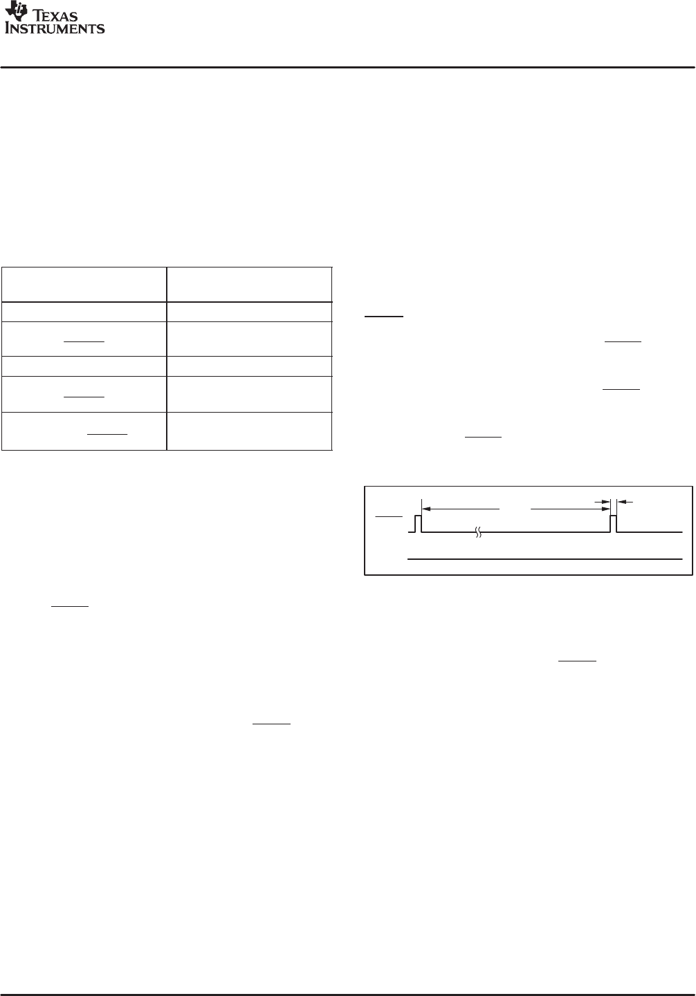
DRDY/FSYNC
In the SPI format, this pin functions as the DRDY output. It
goes low when data is ready for retrieval and then returns
high on the falling edge of the first subsequent SCLK. If data
is not retrieved (that is, SCLK is held low), DRDY
will pulse
high just before the next conversion data is ready, as shown
in Figure 63. The new data is loaded within the ADS1271 one
CLK cycle before DRDY
goes low. All data must be shifted
out before this time to avoid being overwritten.
DRDY
SCLK
1/f
DATA
1/f
CLK
Figure 63. DRDY Timing with No Readback
DOUT
The conversion data is shifted out on DOUT. The MSB
data is valid on DOUT when DRDY
goes low. The
subsequent bits are shifted out with each falling edge of
SCLK. If daisy-chaining, the data shifted in using DIN will
appear on DOUT after all 24 bits have been shifted out.
When the device is configured for modulator output, DOUT
becomes the modulator data output (see the Modulator
Output section).
DIN
This input is used when multiple ADS1271s are to be
daisy-chained together. The DOUT pin of the first device
connects to the DIN pin of the next, etc. It can be used with
either the SPI or Frame-Sync formats. Data is shifted in on
the falling edge of SCLK. When using only one ADS1271,
tie DIN low. See the Daisy-Chaining section for more
information.