
Datasheet


ADS1255
ADS1256
SBAS288K − JUNE 2003 − REVISED SEPTEMBER 2013
www.ti.com
26
System Calibration
System calibration corrects both internal and external
offset and gain errors using the SYSOCAL and SYSGCAL
commands. During system calibration, the appropriate
calibration signals must be applied by the user to the
inputs.
SYSOCAL performs a system offset calibration. The user
must supply a zero input differential signal. The
ADS1255/6 then computes a value that will nullify the
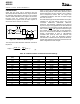
offset in the system. Table 22 shows the time required for
system offset calibration for the different data rate settings.
Note this timing is the same for the self offset calibration.
System offset calibration updates the OFC register.
SYSGCAL performs a system gain calibration. The user
must supply a full-scale input signal to the ADS1255/6.
The ADS1255/6 then computes a value to nullify the gain
error in the system. System gain calibration can correct
inputs that are 80% of the full-scale input voltage and
larger. Make sure not to exceed the full-scale input voltage
when using system gain calibration. Table 22 shows the
time required for system gain calibration for the different
data rate settings. System gain calibration updates the
FSC register.
Table 22. System Gain Calibration Timing
DATA RATE
(SPS)
SYSTEM GAIN CALIBRATION TIME
30,000 417μs
15,000 484μs
7500 617μs
3750 884μs
2000 1.4ms
1000 2.4ms
500 4.4ms
100 20.4ms
60 33.7ms
50 40.4ms
30 67.0ms
25 80.4ms
15 133.7ms
10 200.4ms
5 400.4ms
2.5 800.4ms
NOTE: For f
CLKIN
= 7.68MHz.
Auto-Calibration
Auto-calibration can be enabled (ACAL bit in STATUS
register) to have the ADS1255/6 automatically initiate a
self-calibration at the completion of a write command
(WREG) that changes the data rate, PGA setting, or Buffer
status.
SERIAL INTERFACE
The SPI-compatible serial interface consists of four
signals: CS
, SCLK, DIN, and DOUT, and allows a
controller to communicate with the ADS1255/6. The
programmable functions are controlled using a set of
on-chip registers. Data is written to and read from these
registers via the serial interface
The DRDY
output line is used as a status signal to indicate
when a conversion has been completed. DRDY
goes low
when new data is available. The Timing Specification
shows the timing diagram for interfacing to the
ADS1255/6.
CHIP SELECT (CS)
The chip select (CS) input allows individual selection of a
ADS1255/6 device when multiple devices share the serial
bus. CS must remain low for the duration of the serial
communication. When CS
is taken high, the serial
interface is reset and DOUT enters a high impedance
state. CS may be permanently tied low.
SERIAL CLOCK (SCLK)
The serial clock (SCLK) features a Schmitt-triggered input
and is used to clock data on the DIN and DOUT pins into
and out of the ADS1255/6. Even though the input has
hysteresis, it is recommended to keep SCLK as clean as
possible to prevent glitches from accidentally shifting the
data. If SCLK is held low for 32 DRDY
periods, the serial
interface will reset and the next SCLK pulse will start a new
communication cycle. This timeout feature can be used to
recover communication when a serial interface transmis-
sion is interrupted. A special pattern on SCLK will reset the
chip; see the RESET section for more details on this
procedure. When the serial interface is idle, hold SCLK
low.
DATA INPUT (DIN) AND DATA OUTPUT (DOUT)
The data input pin (DIN) is used along with SCLK to send
data to the ADS1255/6. The data output pin (DOUT) along
with SCLK is used to read data from the ADS1255/6. Data
on DIN is shifted into the part on the falling edge of SCLK
while data is shifted out on DOUT on the rising edge of
SCLK. DOUT is high impedance when not in use to allow
DIN and DOUT to be connected together and be driven by
a bi-directional bus. Note: the RDATAC command must
not be issued while DIN and DOUT are connected
together.