
Datasheet


ADS1251
7
SBAS184D
www.ti.com
THEORY OF OPERATION
The ADS1251 is a precision, high-dynamic range, 24-bit,
delta-sigma, A/D converter capable of achieving very
high-resolution digital results at high data rates. The analog
input signal is sampled at a rate determined by the frequency
of the system clock (CLK). The sampled analog input is
modulated by the delta-sigma A/D modulator, which is fol-
lowed by a digital filter. A Sinc
5
digital low-pass filter processes
the output of the delta-sigma modulator and writes the result
into the data-output register. The DOUT/DRDY
pin is pulled
LOW, indicating that new data are available to be read by the
external microcontroller/microprocessor. As shown in the block
diagram on the front page, the main functional blocks of the
ADS1251 are the 4th-order delta-sigma modulator, a digital
filter, control logic, and a serial interface. Each of these
functional blocks is described in the following sections.
ANALOG INPUT
The ADS1251 contains a fully differential analog input. In
order to provide low system noise, common-mode rejection
of 98dB, and excellent power-supply rejection, the design
topology is based on a fully differential switched-capacitor
architecture. The bipolar input voltage range is from –4.096
to +4.096V, when the reference input voltage equals +4.096V.
The bipolar range is with respect to –V
IN
, and not with respect
to GND.
The differential input impedance of the analog input changes
with the ADS1251 system clock frequency (CLK). The rela-
tionship is:
Impedance (Ω) = (8MHz/CLK) • 210,000
See application note
Understanding the ADS1251, ADS1253,
and ADS1254 Input Circuitry
(SBAA086), available for down-
load from TI’s web site www.ti.com.
With regard to the analog-input signal, the overall analog
performance of the device is affected by three items. First,
the input impedance can affect accuracy. If the source
impedance of the input signal is significant, or if there is
passive filtering prior to the ADS1251, a significant portion of
the signal can be lost across this external impedance. The
magnitude of the effect is dependent on the desired system
performance.
Second, the current into or out of the analog inputs must be
limited. Under no conditions should the current into or out of
the analog inputs exceed 10mA.
Third, to prevent aliasing of the input signal, the bandwidth of
the analog-input signal must be band-limited; the bandwidth
is a function of the system clock frequency. With a system
clock frequency of 8MHz, the data output rate is 20.8kHz with
a –3dB frequency of 4.24kHz. The –3dB frequency scales
with the system clock frequency.
To ensure the best linearity of the ADS1251, and to maxi-
mize the elimination of even-harmonic noise errors, a fully
differential signal is recommended.
For more information about the ADS1251 input structure,
refer to application note SBAA086 found at www.ti.com.
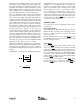
BIPOLAR INPUT
Each of the differential inputs of the ADS1251 must stay
between –0.3V and V
DD
. With a reference voltage at less
than half of V
DD
, one input can be tied to the reference
voltage, and the other input can range from 0V to
2 • V
REF
. By using a three op amp circuit featuring a single
amplifier and four external resistors, the ADS1251 can be
configured to accept bipolar inputs referenced to ground. The
conventional ±2.5V, ±5V, and ±10V input ranges can be
interfaced to the ADS1251 using the resistor values shown in
Figure 1.
FIGURE 1. Level-Shift Circuit for Bipolar Input Ranges.
10kΩ
20kΩ
R
1
OPA4350
OPA4350
OPA4350
+IN
–IN
V
REF
ADS1251
R
2
Bipolar
Input
REF
2.5V
BIPOLAR INPUT R
1
R
2
±10V 2.5kΩ 5kΩ
±5V 5kΩ 10kΩ
±2.5V 10kΩ 20kΩ