
Datasheet


ADS1240, 1241
6
SBAS173F
www.ti.com
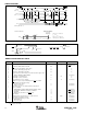
SPEC DESCRIPTION MIN MAX UNITS
t
1
SCLK Period 4t
OSC
Periods
3 DRDY Periods
t
2
SCLK Pulse Width, HIGH and LOW 200 ns
t
3
CS low to first SCLK Edge; Setup Time
(2)
0ns
t
4
D
IN
Valid to SCLK Edge; Setup Time 50 ns
t
5
Valid D
IN
to SCLK Edge; Hold Time 50 ns
t
6
Delay between last SCLK edge for D
IN
and first SCLK edge for D
OUT
:
RDATA, RDATAC, RREG, WREG 50 t
OSC
Periods
t
7
(1)
SCLK Edge to Valid New D
OUT
50 ns
t
8
(1)
SCLK Edge to D
OUT
, Hold Time 0 ns
t
9
Last SCLK Edge to D
OUT
Tri-State 6 10 t
OSC
Periods
NOTE: D
OUT
goes tri-state immediately when CS goes HIGH.
t
10
CS LOW time after final SCLK edge.
Read from the device 0 t
OSC
Periods
Write to the device 8 t
OSC
Periods
t
11
Final SCLK edge of one command until first edge SCLK
of next command:
RREG, WREG, DSYNC, SLEEP, RDATA, RDATAC, STOPC
4t
OSC
Periods
SELFGCAL, SELFOCAL, SYSOCAL, SYSGCAL 2 DRDY Periods
SELFCAL 4 DRDY Periods
RESET (also SCLK Reset or RESET Pin) 16 t
OSC
Periods
t
16
Pulse Width 4t
OSC
Periods
t
17
Allowed analog input change for next valid conversion. 5000 t
OSC
Periods
t
18
DOR update, DOR data not valid. 4 t
OSC
Periods
t
19
First SCLK after DRDY goes LOW:
RDATAC Mode 10 t
OSC
Periods
Any other mode 0 t
OSC
Periods
NOTES: (1) Load = 20pF 10kΩ to DGND.
(2) CS may be tied LOW.
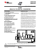
TIMING DIAGRAMS
TIMING CHARACTERISTICS TABLE
t
4
MSB
(Command or Command and Data)
LSB
t
5
t
1
t
3
CS
SCLK
(POL = 0)
D
IN
D
OUT
NOTE: (1) Bit order = 0.
SCLK Reset Waveform
t
7
MSB
(1)
LSB
(1)
t
8
t
10
t
2
t
2
t
11
t
6
t
9
SCLK
(POL = 1)
t
12
t
14
t
15
t
13
t
13
SCLK
ADS1240 or ADS1241
Resets On
Falling Edge
300 • t
OSC
< t
12
< 500 • t
OSC
t
13
: > 5 • t
OSC
550 • t
OSC
< t
14
< 750 • t
OSC
1050 • t
OSC
< t
15
< 1250 • t
OSC
DIAGRAM 1.
DIAGRAM 2.
t
17
t
18
DRDY
SCLK
t
DATA
t
16
RESET, DSYNC, PDWN
t
19