
Datasheet


ADS1210, ADS1211
29
SBAS034B
www.ti.com
The recommended solution to this problem is to actively pull
SDIO LOW. If SDIO is LOW when the ADS1210/11 enters
the instruction byte, then the resulting instruction is a write
of one byte of data to the Data Output Register, which results
in no internal operation.
If the SDIO signal cannot be actively pulled LOW, then
another possibility is to time the initialization of the
controller’s serial port such that it becomes active between
adjacent DRDY LOW periods. The default configuration for
the ADS1210/11 produces a data rate of 814Hz—a conver-
sion period of 1.2ms. This time should be more than ad-
equate for most microcontrollers and DSPs to monitor DRDY
and initialize the serial port at the appropriate time.
Master Mode
The Master Mode is active when the MODE input is HIGH.
All serial clock cycles will be produced by the ADS1210/11
in this mode, and the SCLK pin is configured as an output.
The frequency of the serial clock will be one-half of the X
IN
frequency. Multiple instructions cannot be issued during a
single conversion period in this mode—only one instruction
per conversion cycle is possible.
The Master Mode will be difficult for some microcontrollers,
particularly when the X
IN
input frequency is greater than a
few MHz, as the serial clock may exceed the microcontroller’s
maximum serial clock frequency. For the majority of digital
signal processors, this will be much less of a concern. In
addition, if SDIO is being used as an input and an output,
then the transition time from input to output may be a
concern. This will be true for both microcontrollers and
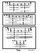
DSPs. See Figure 20 in the Timing section.
Note that if CS is tied LOW, there are special considerations
regarding SDIO as outlined previously in this section. Also
note that if CS is being used to control the flow of data from
the ADS1210/11 and it remains HIGH for one or more
conversion periods, the ADS1210/11 will operate properly.
However, the result in the Data Output Register will be lost
when it is overwritten by each new result. Just prior to this
update, DRDY will be forced HIGH and will return LOW
after the update.
Slave Mode
Most systems will use the ADS1210/11 in the Slave Mode.
This mode allows multiple instructions to be issued per
conversion period as well as allowing the main controller to
set the serial clock frequency and pace the serial data
transfer. The ADS1210/11 is in the Slave Mode when the
MODE input is LOW.
There are several important items regarding the serial clock
for this mode of operation. The maximum serial clock
frequency cannot exceed the ADS1210/11 X
IN
frequency
divided by 5 (see Figure 15 in the Timing section).
When using SDIO as the serial output, the falling edge of the
last serial clock cycle of the instruction byte will cause the
SDIO pin to begin its transition from input to output.
Between three and four X
IN
cycles after this falling edge, the
SDIO pin will become an output. This transition may be too
fast for some microcontrollers and digital signal processors.
Using CS and Continuous Read Mode
The serial interface may make use of the CS signal, or this
input may simply be tied LOW. There are several issues
associated with choosing to do one or the other.
The CS signal does not directly control the tri-state condition
of the SDOUT or SDIO output. These signals are normally
in the tri-state condition. They only become active when
serial data is being transmitted from the ADS1210/11. If the
ADS1210/11 is in the middle of a serial transfer and SDOUT
or SDIO is an output, taking CS HIGH will not tri-state the
output signal.
If there are multiple serial peripherals utilizing the same
serial I/O lines and communication may occur with any
peripheral at any time, then the CS signal must be used. The
ADS1210/11 may be in the Master Mode or the Slave Mode.
In the Master Mode, the CS signal is used to hold-off serial
communication with a “ready” (DRDY LOW) ADS1210/11
until the main controller can accommodate the communica-
tion. In the Slave Mode, the CS signal is used to enable
communication with the ADS1210/11.
The CS input has another use. If the CS state is left LOW
after a read of the Data Output Register has been performed,
then the next time that DRDY goes LOW, the ADS1210/11
Instruction Register will not be entered. Instead, the Instruc-
tion Register contents will be re-used, and the new contents
of the Data Output Register, or some part thereof, will be
transmitted. This will occur as long as CS is LOW and not
toggled.
This mode of operation is called the Continuous Read Mode
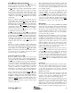
and is shown in the read flowcharts of Figures 25 and 26. It
is also shown in the Timing Diagrams of Figures 18 and 19
in the Timing section. Note that once CS has been taken
HIGH, the Continuous Read Mode will be enabled (but not
entered) and can never be disabled. The mode is actually
entered and exited as described above.
Power-On Conditions for SDIO
Even if the SDIO connection will be used only for input,
there is one important item to consider regarding SDIO. This
only applies when the ADS1210/11 is in the Master Mode
and CS will be tied LOW. At power-up, the serial I/O lines
of most microcontrollers and digital signal processors will be
in a tri-state condition, or they will be configured as inputs.
When power is applied to the ADS1210/11, it will begin
operating as defined by the default condition of the Com-
mand Register (see Table X in the System Configuration
section). This condition defines SDIO as the data output pin.
Since the ADS1210/11 is in the Master Mode and CS is tied
LOW, the serial clock will run whenever DRDY is LOW and
an instruction will be entered and executed. If the SDIO line
is HIGH, as it might be with an active pull-up, then the
instruction is a read operation and SDIO will become an
output every DRDY LOW period—for 32 serial clock cycles.
When the serial port on the main controller is enabled, signal
contention could result.