
Datasheet


ADS1194, ADS1196
ADS1198
www.ti.com
SBAS471C –APRIL 2010– REVISED NOVEMBER 2011
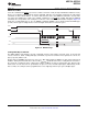
SPI COMMAND DEFINITIONS
The ADS1194/6/8 provide flexible configuration control. The opcode commands, summarized in Table 9, control
and configure the operation of the ADS1194/6/8. The opcode commands are stand-alone, except for the register
read and register write operations that require a second command byte plus data. CS can be taken high or held
low between opcode commands but must stay low for the entire command operation (especially for multi-byte
commands). System opcode commands and the RDATA command are decoded by the ADS1194/6/8 on the
seventh falling edge of SCLK. The register read/write opcodes are decoded on the eighth SCLK falling edge. Be
sure to follow SPI timing requirements when pulling CS high after issuing a command.
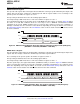
Table 9. Command Definitions
COMMAND DESCRIPTION FIRST BYTE SECOND BYTE
System Commands
WAKEUP Wake-up from standby mode. NOP command in normal mode. 0000 0010 (02h)
STANDBY Enter standby mode 0000 0100 (04h)
RESET Reset the device 0000 0110 (06h)
START Start/restart (synchronize) conversions 0000 1000 (08h)
STOP Stop conversion 0000 1010 (0Ah)
Data Read Commands
Enable Read Data Continuous mode.
RDATAC 0001 0000 (10h)
This mode is the default mode at power-up.
(1)
SDATAC Stop Read Data Continuously mode 0001 0001 (11h)
RDATA Read data by command; supports multiple read back. 0001 0010 (12h)
Register Read Commands
RREG Read n nnnn registers starting at address rrrr 001r rrrr (2xh)
(2)
000n nnnn
(2)
WREG Write n nnnn registers starting at address rrrr 010r rrrr (4xh)
(2)
000n nnnn
(2)
(1) When in RDATAC mode, the RREG command is ignored.
(2) n nnnn = number of registers to be read/written – 1. For example, to read/write three registers, set nnnn = 0 (0010). rrrr = starting
register address for read/write opcodes.
WAKEUP: Exit STANDBY Mode
This opcode exits the low-power standby mode; see the STANDBY: Enter STANDBY Mode subsection of the
SPI Command Definitions section. Time is required when exiting standby mode (see the Electrical
Characteristics for details). There are no restrictions on the SCLK rate for this command and it can be
issued any time. Any following command must be sent after 4 CLK cycles.
STANDBY: Enter STANDBY Mode
This opcode command enters the low-power standby mode. All parts of the circuit are shut down except for the
reference section. The standby mode power consumption is specified in the Electrical Characteristics. There are
no restrictions on the SCLK rate for this command and it can be issued any time.
RESET: Reset Registers to Default Values
This command resets the digital filter cycle and returns all register settings to the default values. See the Reset
(RESET) subsection of the SPI Interface section for more details. There are no restrictions on the SCLK rate
for this command and it can be issued any time. It takes 18 CLK cycles to execute the RESET command.
Avoid sending any commands during this time.
START: Start Conversions
This opcode starts data conversions. Tie the START pin low to control conversions by command. If conversions
are in progress this command has no effect. The STOP opcode command is used to stop conversions. If the
START command is immediately followed by a STOP command then have a gap of 4 CLK cycles between them.
When the START opcode is sent to the device, keep the START pin low until the STOP command is issued.
(See the START subsection of the SPI Interface section for more details.) There are no restrictions on the
SCLK rate for this command and it can be issued any time.
Copyright © 2010–2011, Texas Instruments Incorporated Submit Documentation Feedback 35
Product Folder Link(s): ADS1194 ADS1196 ADS1198