
Datasheet


S
SN
S
N
SN
N
C
P
tt
t
P
tt
t
P
+
+
=
xx
+
ADC128S052
SNAS333D –AUGUST 2005–REVISED MARCH 2013
www.ti.com
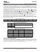
Figure 39. Power Consumption Equation
Power Supply Noise Considerations
The charging of any output load capacitance requires current from the digital supply, V
D
. The current pulses
required from the supply to charge the output capacitance will cause voltage variations on the digital supply. If
these variations are large enough, they could degrade SNR and SINAD performance of the ADC. Furthermore, if
the analog and digital supplies are tied directly together, the noise on the digital supply will be coupled directly
into the analog supply, causing greater performance degradation than would noise on the digital supply alone.
Similarly, discharging the output capacitance when the digital output goes from a logic high to a logic low will
dump current into the die substrate, which is resistive. Load discharge currents will cause "ground bounce" noise
in the substrate that will degrade noise performance if that current is large enough. The larger the output
capacitance, the more current flows through the die substrate and the greater the noise coupled into the analog
channel.
The first solution to keeping digital noise out of the analog supply is to decouple the analog and digital supplies
from each other or use separate supplies for them. To keep noise out of the digital supply, keep the output load
capacitance as small as practical. If the load capacitance is greater than 50 pF, use a 100 Ω series resistor at
the ADC output, located as close to the ADC output pin as practical. This will limit the charge and discharge
current of the output capacitance and improve noise performance. Since the series resistor and the load
capacitor form a low frequency pole, verify signal integrity once the series resistor has been added.
LAYOUT AND GROUNDING
Capacitive coupling between the noisy digital circuitry and the sensitive analog circuitry can lead to poor
performance. The solution is to keep the analog circuitry separated from the digital circuitry and the clock line as
short as possible.
Digital circuits create substantial supply and ground current transients. The logic noise generated could have
significant impact upon system noise performance. To avoid performance degradation of the ADC128S052 due
to supply noise, do not use the same supply for the ADC128S052 that is used for digital logic.
Generally, analog and digital lines should cross each other at 90° to avoid crosstalk. However, to maximize
accuracy in high resolution systems, avoid crossing analog and digital lines altogether. It is important to keep
clock lines as short as possible and isolated from ALL other lines, including other digital lines. In addition, the
clock line should also be treated as a transmission line and be properly terminated.
The analog input should be isolated from noisy signal traces to avoid coupling of spurious signals into the input.
Any external component (e.g., a filter capacitor) connected between the converter's input pins and ground or to
the reference input pin and ground should be connected to a very clean point in the ground plane.
We recommend the use of a single, uniform ground plane and the use of split power planes. The power planes
should be located within the same board layer. All analog circuitry (input amplifiers, filters, reference
components, etc.) should be placed over the analog power plane. All digital circuitry and I/O lines should be
placed over the digital power plane. Furthermore, all components in the reference circuitry and the input signal
chain that are connected to ground should be connected together with short traces and enter the analog ground
plane at a single, quiet point.
18 Submit Documentation Feedback Copyright © 2005–2013, Texas Instruments Incorporated
Product Folder Links: ADC128S052