
Datasheet


ABC
CH0
CH1
CH2
CH3
CH4
CH5
CH6
CH7
COM
MUXOUT1
A/DIN1
MUXOUT2
A/DIN2
DGND
V
D
+
CCLK
SCLK
DI
DO
EOC
PD
AGND
VREF+
VREF-
V
A
+
DOR
CS
CONV
RS-232
Interface
+4.096V
+5V
D Q
CLK
7474
1/6 74HC04
1/4 DS14C89
1/4 DS14C89
1/4 DS14C88
+5V
5 MHz
DTR
RTS
CTS
ADC12130, ADC12132, ADC12138
www.ti.com
SNAS098G –MARCH 2000–REVISED MARCH 2013
As an example, this device with a differential signed 5V, 1 kHz sine wave input signal will typically have a S/(N +
D) of 77 dB, which is equivalent to 12.5 effective bits.
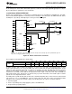
15.0 AN RS232 SERIAL INTERFACE
Shown on the following page is a schematic for an RS232 interface to any IBM and compatible PCs. The DTR,
RTS, and CTS RS232 signal lines are buffered via level translators and connected to the ADC12138's DI, SCLK,
and DO pins, respectively. The D flip-flop is used to generate the CS signal.
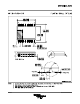
Note: V
A
+
, V
D
+
, and V
REF
+
on the ADC12138 each have 0.01 μF and 0.1 μF chip caps, and 10 μF tantalum caps. All
logic devices are bypassed with 0.1 μF caps.
Figure 76. RS232 Serial Interface Schematic
The assignment of the RS232 port is shown below
B7 B6 B5 B4 B3 B2 B1 B0
Input Address 3FE X X X CTS X X X X
COM1
Output Address 3FC X X X 0 X X RTS DTR
A sample program, written in Microsoft QuickBasic, is shown on the next page. The program prompts for data
mode select instruction to be sent to the ADC. This can be found from the Mode Programming table shown
earlier. The data should be entered in “1”s and “0”s as shown in the table with DI0 first. Next, the program
prompts for the number of SCLK cycles required for the programmed mode select instruction. For instance, to
send all “0”s to the ADC, selects CH0 as the +input, CH1 as the −input, 12-bit conversion, and 13-bit MSB first
data output format (if the sign bit was not turned off by a previous instruction). This would require 13 SCLK
periods since the output data format is 13 bits.
The ADC powers up with No Auto Cal, No Auto Zero, 10 CCLK Acquisition Time, 12-bit conversion, data out with
sign, power up, 12- or 13-bit MSB First, and user mode. Auto Cal, Auto Zero, Power Up and Power Down
instructions do not change these default settings. The following power up sequence should be followed:
1. Run the program
2. Prior to responding to the prompt apply the power to the ADC12138
3. Respond to the program prompts
Copyright © 2000–2013, Texas Instruments Incorporated Submit Documentation Feedback 41
Product Folder Links: ADC12130 ADC12132 ADC12138