
Datasheet


DV
DD
DV
SS
1
ADC1175
www.ti.com
SNAS012H –JANUARY 2000–REVISED APRIL 2013
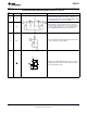
PIN DESCRIPTIONS AND EQUIVALENT CIRCUITS (continued)
Pin
Symbol Equivalent Circuit Description
No.
Analog Input that is the high (top) side of the reference ladder
of the ADC. Nominal range is 1.0V to AV
DD
. Voltage on V
RT
17 V
RT
and V
RB
inputs define the V
IN
conversion range. Bypass well.
See REFERENCE INPUTS for more information.
Analog Input that is the low (bottom) side of the reference
ladder of the ADC. Nominal range is 0V to 4.0V. Voltage on
23 V
RB
V
RT
and V
RB
inputs define the V
IN
conversion range. Bypass
well. See REFERENCE INPUTS for more information.
Reference Bottom Bias with internal pull down resistor. Short
22 V
RBS
to V
RB
to self bias the reference ladder.
CMOS/TTL compatible Digital input that, when low, enables
1 OE the digital outputs of the ADC1175. When high, the outputs
are in a high impedance state.
Copyright © 2000–2013, Texas Instruments Incorporated Submit Documentation Feedback 3
Product Folder Links: ADC1175