
Datasheet


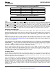


Table Of Contents
- Features
- Applications
- Key Specifications
- Description
- Absolute Maximum Ratings
- Operating Ratings
- Package Thermal Resistance
- Converter Characteristics
- DC Electrical Characteristics
- AC Electrical Characteristics
- TRI-STATE Test Circuits and Waveforms
- Typical Performance Characteristics
- Functional Description
- Revision History

ADC10662, ADC10664
SNAS076E –JUNE 1999–REVISED MARCH 2013
www.ti.com
Figure 19. Block Diagram of the Multistep Converter Architecture
SIMILAR PRODUCT DIFFERENCES
The ADC1006x, ADC1046x and ADC1066x (where "x" indicates the number of multiplexer inputs) are similar
devices with different specification limits. The differences in these device families are summarized below.
Device Family ILE, TUE, PSS THD, SNR, ENOB Max. Conversion Time
ADC1006x Verified - 900ns
ADC1046x - Verified 900ns
ADC1066x - Verified 466ns
Applications Information
MODES OF OPERATION
The ADC10662 and ADC10664 have two basic digital interface modes. Figure 3 and Figure 4 are timing
diagrams for the two modes. The ADC10662 and ADC10664 have input multiplexers that are controlled by the
logic levels on pins S
0
and S
1
when S/H goes low. Table 1 and Table 2 are truth tables showing how the input
channels are assigned.
Mode 1
In this mode, the S/H pin controls the start of conversion. S/H is pulled low for a minimum of 150 ns. This causes
the comparators in the “coarse” flash converter to become active. When S/H goes high, the result of the coarse
conversion is latched and the “fine” conversion begins. After 360 ns (typical), INT goes low, indicating that the
conversion results are latched and can be read by pulling RD low. Note that CS must be low to enable S/H or
RD. CS is internally “ANDed” with S/H and RD; the input voltage is sampled when CS and S/H are low, and data
is read when CS and RD are low. INT is reset high on the rising edge of RD.
12 Submit Documentation Feedback Copyright © 1999–2013, Texas Instruments Incorporated
Product Folder Links: ADC10662 ADC10664