
Datasheet


501-325
Rev A 2 of 4
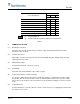
1.6. Test Sequence
Test or Examination
Test Group (a)
123
Test Sequence (b)
Examination of product 1,3,5 1,3 1,8
Insulation resistance 2,6
Withstanding voltage 3,7
Solderability 2
Component resistance to wave soldering 2
Contact retention 4
Thermal shock 4
Humidity/temperature cycling 5
(a) See paragraph 1.4.
NOTE
(b) Numbers indicate sequence in which tests are performed.
Figure 2
2. SUMMARY OF TESTING
2.1. Examination of Product
Specimens were visually examined and no evidence of physical damage detrimental to product
performance was observed.
2.2. Insulation Resistance
All insulation resistance measurements were greater than 5000 megohms initially, and greater than
1000 megohms after testing.
2.3. Withstanding Voltage
No dielectric breakdown or flashover occurred.
2.4. Solderability
All contact leads had a minimum of 95% solder coverage.
2.5. Component Resistance to Wave Soldering
No specimen exhibited any visual evidence of blistering, warpage, or significant discoloration. Slight
discoloration was observed around the contacts as viewed from the bottom of the connectors using a
microscope. No discoloration or other anomalies were observed when viewing the connectors from the
inside.
2.6. Contact Retention
No physical damage occurred to either the contacts or the housing as a result applying an axial load to
the contacts for 6 seconds.