
Datasheet


Electrical characteristics STM32F103x4, STM32F103x6
72/99 DocID15060 Rev 7
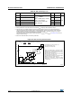
Figure 34. ADC accuracy characteristics
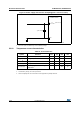
Table 49. ADC accuracy
(1)
(2)
(3)
1. ADC DC accuracy values are measured after internal calibration.
2. Better performance could be achieved in restricted V
DD
, frequency and temperature ranges.
3. ADC Accuracy vs. Negative Injection Current: Injecting negative current on any of the standard (non-
robust) analog input pins should be avoided as this significantly reduces the accuracy of the conversion
being performed on another analog input. It is recommended to add a Schottky diode (pin to ground) to
standard analog pins which may potentially inject negative current.
Any positive injection current within the limits specified for I
INJ(PIN)
and ΣI
INJ(PIN)
in Section 5.3.12 does not
affect the ADC accuracy.
Symbol Parameter Test conditions Typ Max
(4)
4. Based on characterization, not tested in production.
Unit
ET
Total unadjusted error
f
PCLK2
= 56 MHz,
f
ADC
= 14 MHz, R
AIN
< 10 kΩ,
V
DDA
= 2.4 V to 3.6 V
Measurements made after
ADC calibration
±2 ±5
LSB
EO
Offset error ±1.5 ±2.5
EG
Gain error ±1.5 ±3
ED
Differential linearity error ±1 ±2
EL
Integral linearity error ±1.5 ±3
E
O
E
G
1LSB
IDEAL
(1) Example of an actual transfer curve
(2) The ideal transfer curve
(3) End point correlation line
E
T
=Total Unadjusted Error: maximum deviation
between the actual and the ideal transfer curves.
E
O
=Offset Error: deviation between the first actual
transition and the first ideal one.
E
G
=Gain Error: deviation between the last ideal
transition and the last actual one.
E
D
=Differential Linearity Error: maximum deviation
between a ctual steps and the ideal one.
E
L
=Integral Linearity Error: maximum deviation
between any actual transition and the end point
correlation line.
4095
4094
4093
5
4
3
2
1
0
7
6
123 4567
4093 4094 4095 4096
(1)
(2)
E
T
E
D
E
L
(3)
V
DDA
V
SSA
ai14395b
V
REF+
4096
(or depending on package)]
V
DDA
4096
[1LSB
IDEAL
=