
Datasheet


DocID12943 Rev 14 17/47
M24M01-R M24M01-DF Instructions
46
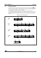
5.1.3 Write Identification Page (M24M01-D only)
The Identification Page (256 byte) is an additional page which can be written and (later)
permanently locked in Read-only mode. It is written by issuing the Write Identification Page
instruction. This instruction uses the same protocol and format as Page Write (into memory
array), except for the following differences:
• Device type identifier = 1011b
• MSB address bits A16/A8 are don't care except for address bit A10 which must be ‘0’.
LSB address bits A7/A0 define the byte address inside the Identification page.
If the Identification page is locked, the data bytes transferred during the Write Identification
Page instruction are not acknowledged (NoAck).
5.1.4 Lock Identification Page (M24M01-D only)
The Lock Identification Page instruction (Lock ID) permanently locks the Identification page
in Read-only mode. The Lock ID instruction is similar to Byte Write (into memory array) with
the following specific conditions:
• Device type identifier = 1011b
• Address bit A10 must be ‘1’; all other address bits are don't care
• The data byte must be equal to the binary value xxxx xx1x, where x is don't care
5.1.5 ECC (Error Correction Code) and Write cycling
(1)
The Error Correction Code (ECC) is an internal logic function which is transparent for the
I
2
C communication protocol.
The ECC logic is implemented on each group of four EEPROM bytes
(2)
. Inside a group, if a
single bit out of the four bytes happens to be erroneous during a Read operation, the ECC
detects this bit and replaces it with the correct value. The read reliability is therefore much
improved.
Even if the ECC function is performed on groups of four bytes, a single byte can be
written/cycled independently. In this case, the ECC function also writes/cycles the three
other bytes located in the same group
(2)
. As a consequence, the maximum cycling budget is
defined at group level and the cycling can be distributed over the 4 bytes of the group: the
sum of the cycles seen by byte0, byte1, byte2 and byte3 of the same group must remain
below the maximum value defined
Table 10: Cycling performance.
1. Only for devices identified with process letter K
2.A group of four bytes is located at addresses [4*N, 4*N+1, 4*N+2, 4*N+3], where N is an integer.