
User's Manual

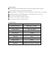


Pin Name Pin Number Description
GND 1 Ground
PIO4 2
PIO5 3
PIO6 4
PIO7 5
PIO8 6
Programmable input/output line
AIO1 7
AIO0 8
Analogue programmable input/output
RESET 9 System Reset(Low Active)
GND 10 Ground
GND 11 Ground
PIO10 12
PIO11 13
PIO12 14
PIO13 15
Programmable input/output line
GND 16 Ground
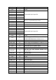
VDD
17
Positive supply for SPI/PCM ports and PIO[15:4]
and BC05 MM Flash Pads, Connect to 3.3V
GND 18 Ground
VDD_Flash 19 Positive supply for Flash Memory ,Connect to 3.3V
VDD_USB 20 Positive supply for UART/USB ports
+1.8V 21 Switch-mode power regulator output
GND 22 Ground
USB_DP 23
USB data plus with selectable internal 1.5k Ω
pull-up resistor
USB_DN 24 USB data minus
WP# 25 Flash write protect(Low Active)
GND 26 Ground
UART_RX 27 UART data input
UART_TX 28 UART data output
PCM_IN 29 Synchronous data input
PCM_SYNC 30 Synchronous data sync
PCM_CLK 31 Synchronous data clock
PCM_OUT 32 Synchronous data output
SPI_CSB 33 Chip select for SPI, active low
SPI_MOSO 34 SPI data output
SPI_CLK 35 SPI clock