
Service manual


LC-20B1U
17
No
. Pin name Function
1 V HOLD
2 HLF
3 MAIN SW
4 TIMELED
5 M/S OUT
6 CSYNC
7 IREMI
8 GND
9 GND
10 XCIN
11 XOUT
12 RESET
13 XOUT
14 GND
15 XIN
16 VCC
17 OSCIN
18 OSCOUT
19 PSWIN
20 SUBREADY
21 BLK
22
23 DAC1CS
24 DAC2CS
25 D SW
26 DTV
27 MRDY
28 SCL2
29 SCL1
30 SDA1
31 SDA2
32 R
33 G
34 B
35 SUBD OUT
36 SUBDIN
37 SUBCLK
38
39 MRDY OUT
40 FCH
41 IREM OUT
42 L_ERR
43 S IN/OUT
44 N443
45 PAL
46 SECAM
47 PAL_M
48 N358
49 PXOE
50 VSH OUT
No
. Pin name Function
51 REQ
52 AV/SY/DY2
53 FSMUTE
54 RSMUTE
55 HPDET
56 SSTBY
57 VSH IN
58 LMUTE
59 V IN/OUT
60 SRESET
61 DENKA
62 VCC
63 CARDPOW
64 VSS
65 TV/AV1
66 AV/AV2
67 VIS/3DS
68 AV1/VISY
69 AV/SY/DY1
70 STD
71 PMUTE
72 POWOUT
73 AD POW
74 IREM 2
75 MPRCS
76 MPRDA
77 MPCS
78 MPDA
79 MPCLK
80 DDCRESET
81 KEY4
82 KEY5
83 CARDRESET
84 SAW SW
85 MODE1
86 MODE2
87 SSYSTEM
88 SSW
89 AFT
90 AGC
91 KEY1
92 KEY2
93 KEY3
94 POWIN
95 VSYNC
96 AVSS
97 HSYNC
98 TVSETB
99 AVCC
100
CVIN
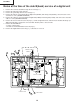
Pin functions of microprocessor IC (IC2001) RH-iXA276WJZZQ
Closed caption
Closed caption
Main switch ON[H]/OFF[L]
Off timer LED light-up
Sub-microprocessor master/slave output
Composite sync signal
Remote control
Grounding
Grounding
32kHz oscillation input
32kHz oscillation output
Reset at “L” level
Microprocessor oscillator connection
Grounding
Microprocessor oscillator connection
Power
OSD clock input
OSD clock output
Main power input
Sub-microprocessor ready input
OSD blanking output
DAC1 chip select
DAC2 chip select
D terminal connection detect
D terminal control line
I
2
C bus open/closed select input
I
2
C bus serial clock line 2
I
2
C bus serial clock line 1
I
2
C bus serial data line 1
I
2
C bus serial data line 2
R signal output
G signal output
B signal output
Sub-microprocessor data output
Sub-microprocessor data input
Sub-microprocessor clock input
I
2
C bus open/closed output
No-signal field ID signal output
Not used
Fluorescent lamp error detect input
Audio input/output select
“H” for N443, “L” for others
“H” for PAL, “L” for others
“H” for SECAM, “L” for others
“H” for PAL-M, “L” for others
“H” for N358, “L” for others
Card (Card mode at “L” level)
Panel gate driver voltage control
Adjustment process
US CCD input select
Front mute
Rear mute
Headphone detect at “L” level
Speaker standby (at “H” level)
Panel gate driver voltage check
Line out audio mute
Video input/output select
Multiplex reset at “L” level
Electric charge prevention
Power
Card (ON/OFF)
Grounding
Analog switch 1
Analog switch 2
Analog switch 3
Analog switch 4
US CCD input select 2
Microprocessor power off output
P mute
DC/DC control output
Adaptor ON/OFF input
Reception at slave
G/A read enable
G/A data input
G/A chip select
G/A data output
G/A clock
Digital decoder reset
Key input 4
Key input 5
Card reset (at “H” level)
Tuner select (at “H” level)
Tuner select (at “H” level)
Tuner select (at “H” level)
S system switching detect
S terminal connect input at “L” level
AFT voltage input
AGC voltage input
Key input 1
Key input 2
Key input 3
DC/DC start-up detect
OSD vertical sync signal
Analog power input (GND)
OSD vertical sync signal
Closed caption (GND)
OSD power input
Closed caption signal input