
Service manual


24
32JW-73E
TDA9886 (IC201)
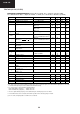
7 PINNING
SYMBOL
PIN
DESCRIPTION
TDA9886T
TDA9886TS
TDA9885T
TDA9885TS
TDA9885HN
VIF1 1 1 30 VIF differential input 1
VIF2 2 2 31 VIF differential input 2
n.c. −−32 not connected
OP1 3 3 1 output port 1; open-collector
FMPLL 4 4 2 FM-PLL for loop filter
DEEM 5 5 3 de-emphasis output for capacitor
AFD 6 6 4 AF decoupling input for capacitor
DGND 7 7 5 digital ground
n.c. −−6 not connected
AUD 8 8 7 audio output
TOP 9 9 8 tuner AGC TakeOver Point (TOP) for resistor adjustment
SDA 10 10 9 I
2
C-bus data input and output
SCL 11 11 10 I
2
C-bus clock input
SIOMAD 12 12 11 sound intercarrier output and MAD select with resistor
n.c. −−12 not connected
n.c. 13 13 13 not connected
n.c. −−14 not connected
TAGC 14 14 15 tuner AGC output
REF 15 15 16 4 MHz crystal or reference signal input
VAGC 16 −−VIF-AGC for capacitor
n.c. − 16 17 not connected
CVBS 17 17 18 composite video output
n.c. −−19 not connected
AGND 18 18 20 analog ground
VPLL 19 19 21 VIF-PLL for loop filter
V
P
20 20 22 supply voltage
AFC 21 21 23 AFC output
OP2 22 22 24 output port 2; open-collector
n.c. −−25 not connected
SIF1 23 23 26 SIF differential input 1 and MAD select with resistor
SIF2 24 24 27 SIF differential input 2 and MAD select with resistor
n.c. −−28 not connected
n.c. −−29 not connected
handbook, halfpage
TDA9885TS
TDA9886TS
MHC110
VIF1
VIF2
OP1
FMPLL
DEEM
AFD
DGND
AUD
TOP
SDA
SCL
SIOMAD
SIF2
SIF1
OP2
AFC
V
P
VPLL
AGND
CVBS
VAGC
(1)
REF
TAGC
n.c.
1
2
3
4
5
6
7
8
9
10
11
12
24
23
22
21
20
19
18
17
16
15
14
13
Fig.3 Pin configuration for SSOP24.
(1) Not connected for TDA9885TS.