
Service manual


22
32JW-73E
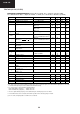
TDA9886 (IC201)
Notes
1. Values of video and sound parameters can be decreased at V
P
= 4.5 V.
2. For applications without I
2
C-bus, the time constant (R × C) at the supply must be >1.2 µs (e.g. 1 Ω and 2.2 µF).
3. Condition: luminance range (5 steps) from 0% to 100%.
4. AC load: C
L
< 20 pF and R
L
>1kΩ. The sound carrier frequencies (depending on the TV standard) are attenuated
by the integrated sound carrier traps (see Figs 13 to 18; H (s) is the absolute value of transfer function).
5. S/N
W(video)
is the ratio of the black-to-white amplitude to the black level noise voltage (RMS value measured on
pin CVBS). B = 5 MHz weighted in accordance with
“CCIR 567”
.
6. Conditions: video signal, grey level, positive and negative modulation.
7. The intercarrier output signal at pin SIOMAD can be calculated by the following formula taking into account the
internal video signal with 1.1 V (p-p) as a reference:
(RMS), where: is the correction term for RMS value,
is the sound-to-picture carrier ratio at pins VIF1 and VIF2 in dB, 6 dB is the correction term of internal
circuitry and ±3 dB is the tolerance of video output and intercarrier output V
o(intc)(rms)
.
8. Pin REF is able to operate as a 1-pin crystal oscillator input as well as an external reference signal input, e.g. from
the tuning system.
B
AF(−3dB)
−3 dB AF bandwidth without de-emphasis;
dependent on FM-PLL filter
80 100 − kHz
S/N
W(AF)
weighted signal-to-noise ratio of
audio signal
FM: 27 kHz FM deviation;
50 µs de-emphasis;
vision carrier unmodulated
52 56 − dB
AM: m = 54% 45 50 − dB
α
AM(sup)
AM suppression of
FM demodulator
50 µs de-emphasis;
AM: f = 1 kHz and m = 54%;
referenced to 27 kHz
FM deviation
40 46 − dB
PSRR
AUD
power supply ripple rejection on
pin AUD
f
ripple
= 70 Hz; see Fig.6
for AM 20 26 − dB
for FM 14 20 − dB
V
o(intc)(rms)
IF intercarrier output level
(RMS value)
QSS mode; SC
1
;SC
2
off 90 140 180 mV
L standard;
without modulation
90 140 180 mV
intercarrier mode;
SC
1
;SC
2
off; note 7
−−−mV
Reference frequency
f
ref
reference signal frequency note 8 − 4 − MHz
V
ref(rms)
reference signal voltage
(RMS value)
operation as input terminal 80 − 400 mV
SYMBOL PARAMETER CONDITIONS MIN. TYP. MAX. UNIT
V
o(intc)
1.1 V (p-p)
1
22
-----------
× 10
V
iSC()
V
iPC()
---------------
dB()6 dB 3 dB±+
20
----------------------------------------------------------------
×=
1
22
-----------
V
iSC()
V
iPC()
---------------
dB()