Rev. 1.0, Sep. 2010 M391B5773DH0 M391B5273DH0 240pin Unbuffered DIMM based on 2Gb D-die 1.35V 78FBGA with Lead-Free & Halogen-Free (RoHS compliant) datasheet SAMSUNG ELECTRONICS RESERVES THE RIGHT TO CHANGE PRODUCTS, INFORMATION AND SPECIFICATIONS WITHOUT NOTICE. Products and specifications discussed herein are for reference purposes only. All information discussed herein is provided on an "AS IS" basis, without warranties of any kind.
Unbuffered DIMM Rev. 1.0 datasheet DDR3L SDRAM Revision History Revision No. 1.0 History - First Release -2- Draft Date Remark Editor Sep. 2010 - S.H.
Unbuffered DIMM datasheet Rev. 1.0 DDR3L SDRAM Table Of Contents 240pin Unbuffered DIMM based on 2Gb D-die 1. DDR3L Unbuffered DIMM Ordering Information ........................................................................................................... 4 2. Key Features................................................................................................................................................................. 4 3. Address Configuration .........................................
Rev. 1.0 datasheet Unbuffered DIMM DDR3L SDRAM 1. DDR3L Unbuffered DIMM Ordering Information Part Number2 Density Organization Number of Rank Component Composition Height M391B5773DH0-YF8/H9/K0 2GB 256Mx64 256Mx8(K4B2G0846D-HY##)*9 1 30mm M391B5273DH0-YF8/H9/K0 4GB 512Mx72 256Mx8(K4B2G0846D-HY##)*18 2 30mm NOTE : 1. "##" - F8/H9/K0 2.
Rev. 1.0 datasheet Unbuffered DIMM DDR3L SDRAM 4.
Rev. 1.0 datasheet Unbuffered DIMM DDR3L SDRAM 5.
datasheet Unbuffered DIMM Rev. 1.0 DDR3L SDRAM 7. Input/Output Functional Description Symbol Type Function CK0-CK1 CK0-CK1 SSTL CK and CK are differential clock inputs. All the DDR3 SDRAM addr/cntl inputs are sampled on the crossing of positive edge of CK and negative edge of CK. Output (read) data is reference to the crossing of CK and CK (Both directions of crossing) CKE0-CKE1 SSTL Activates the SDRAM CK signal when high and deactivates the CK signal when low.
datasheet Unbuffered DIMM Rev. 1.0 DDR3L SDRAM 7.1 Address Mirroring Feature There is a via grid located under the DRAMs for wiring the CA signals (address, bank address, command, and control lines) to the DRAM pins. The length of the traces from the vias to the DRAMs places limitations on the bandwidth of the module. The shorter these traces, the higher the bandwidth. To extend the bandwidth of the CA bus for DDR3 modules, a scheme was defined to reduce the length of these traces.
Rev. 1.0 datasheet Unbuffered DIMM DDR3L SDRAM 8. Function Block Diagram: 8.
Rev. 1.0 datasheet Unbuffered DIMM DDR3L SDRAM 8.
Rev. 1.0 datasheet Unbuffered DIMM DDR3L SDRAM 9. Absolute Maximum Ratings 9.1 Absolute Maximum DC Ratings Symbol Parameter Rating Units NOTE VDD Voltage on VDD pin relative to VSS -0.4 V ~ 1.975 V V 1,3 VDDQ Voltage on VDDQ pin relative to VSS -0.4 V ~ 1.975 V V 1,3 VIN, VOUT Voltage on any pin relative to VSS -0.4 V ~ 1.975 V V 1 TSTG Storage Temperature -55 to +100 °C 1, 2 NOTE : 1.
Rev. 1.0 datasheet Unbuffered DIMM DDR3L SDRAM 11. AC & DC Input Measurement Levels 11.1 AC & DC Logic Input Levels for Single-ended Signals [ Table 2 ] Single Ended AC and DC input levels for Command and Address Symbol Parameter DDR3-800/1066/1333/1600 Min. Max. Unit NOTE 1.35V VIH.CA(DC90) DC input logic high VREF + 90 VDD mV 1,5a) VIL.CA(DC90) DC input logic low VSS VREF - 90 mV 1,6a) VIH.CA(AC160) AC input logic high VREF + 160 Note 2 mV 1,2 VIL.
Rev. 1.0 datasheet Unbuffered DIMM DDR3L SDRAM [ Table 3 ] Single Ended AC and DC input levels for DQ and DM Symbol Parameter DDR3-800/1066 Min. DDR3-1333/1600 Max. Min. Max. Unit NOTE 1.35V VIH.DQ(DC90) DC input logic high VREF + 90 VDD VREF + 90 VDD mV 1,5a) VSS VREF - 90 VSS VREF - 90 mV 1,6a) VIH.DQ(AC160) AC input logic high VREF + 160 Note 2 - - mV 1,2 VIL.DQ(AC160) AC input logic low Note 2 VREF - 160 - - mV 1,2 VIH.
Rev. 1.0 datasheet Unbuffered DIMM DDR3L SDRAM 11.2 VREF Tolerances The dc-tolerance limits and ac-noise limits for the reference voltages VREFCA and VREFDQ are illustrate in Figure 2. It shows a valid reference voltage VREF(t) as a function of time. (VREF stands for VREFCA and VREFDQ likewise). VREF(DC) is the linear average of VREF(t) over a very long period of time (e.g. 1 sec). This average has to meet the min/max requirements of VREF.
Rev. 1.0 datasheet Unbuffered DIMM DDR3L SDRAM 11.3 AC and DC Logic Input Levels for Differential Signals 11.3.1 Differential Signals Definition tDVAC Differential Input Voltage (i.e. DQS-DQS, CK-CK) VIH.DIFF.AC.MIN VIH.DIFF.MIN 0.0 half cycle VIL.DIFF.MAX VIL.DIFF.AC.MAX tDVAC time Figure 3. Definition of differential ac-swing and "time above ac level" tDVAC 11.3.2 Differential Swing Requirement for Clock (CK - CK) and Strobe (DQS - DQS) DDR3-800/1066/1333/1600 Symbol Parameter 1.35V 1.
Unbuffered DIMM Rev. 1.0 datasheet DDR3L SDRAM [ Table 4 ] Allowed time before ringback (tDVAC) for CK - CK and DQS - DQS (1.35V) Slew Rate [V/ns] tDVAC [ps] @ |VIH/Ldiff(AC)| = 320mV tDVAC [ps] @ |VIH/Ldiff(AC)| = 270mV min max min max > 4.0 TBD - TBD - 4.0 TBD - TBD - 3.0 TBD - TBD - 2.0 TBD - TBD - 1.8 TBD - TBD - 1.6 TBD - TBD - 1.4 TBD - TBD - 1.2 TBD - TBD - 1.0 TBD - TBD - < 1.
Rev. 1.0 datasheet Unbuffered DIMM DDR3L SDRAM 11.3.3 Single-ended Requirements for Differential Signals Each individual component of a differential signal (CK, DQS, CK, DQS) has also to comply with certain requirements for single-ended signals. CK and CK have to approximately reach VSEHmin / VSELmax (approximately equal to the ac-levels ( VIH(AC) / VIL(AC) ) for ADD/CMD signals) in every half-cycle.
Rev. 1.0 datasheet Unbuffered DIMM DDR3L SDRAM 11.3.4 Differential Input Cross Point Voltage To guarantee tight setup and hold times as well as output skew parameters with respect to clock and strobe, each cross point voltage of differential input signals (CK, CK and DQS, DQS) must meet the requirements in below table. The differential input cross point voltage VIX is measured from the actual cross point of true and complement signal to the mid level between of VDD and VSS.
Rev. 1.0 datasheet Unbuffered DIMM DDR3L SDRAM 11.4 Slew Rate Definition for Single Ended Input Signals See "Address / Command Setup, Hold and Derating" for single-ended slew rate definitions for address and command signals. See "Data Setup, Hold and Slew Rate Derating" for single-ended slew rate definitions for data signals. 11.5 Slew rate definition for Differential Input Signals Input slew rate for differential signals (CK, CK and DQS, DQS) are defined and measured as shown in below.
Rev. 1.0 datasheet Unbuffered DIMM DDR3L SDRAM 12.3 Single-ended Output Slew Rate With the reference load for timing measurements, output slew rate for falling and rising edges is defined and measured between VOL(AC) and VOH(AC) for single ended signals as shown in below.
Rev. 1.0 datasheet Unbuffered DIMM DDR3L SDRAM 12.4 Differential Output Slew Rate With the reference load for timing measurements, output slew rate for falling and rising edges is defined and measured between VOLdiff(AC) and VOHdiff(AC) for differential signals as shown in below.
Unbuffered DIMM datasheet Rev. 1.0 DDR3L SDRAM 13. IDD specification definition Symbol Description IDD0 Operating One Bank Active-Precharge Current CKE: High; External clock: On; tCK, nRC, nRAS, CL: Refer to Component Datasheet for detail pattern ; BL: 81); AL: 0; CS: High between ACT and PRE; Command, Address, Bank Address Inputs: partially toggling ; Data IO: FLOATING; DM:stable at 0; Bank Activity: Cycling with one bank active at a time: 0,0,1,1,2,2,...
Unbuffered DIMM datasheet Rev. 1.
Rev. 1.0 datasheet Unbuffered DIMM DDR3L SDRAM 14. IDD SPEC Table M391B5773DH0 : 2GB(256Mx72) Module DDR3-1066 Symbol DDR3-1333 7-7-7 DDR3-1600 9-9-9 11-11-11 Unit NOTE 405 mA 1 495 mA 1 1.35V 1.5V 1.35V 1.5V 1.35V 1.
Rev. 1.0 datasheet Unbuffered DIMM DDR3L SDRAM 15. Input/Output Capacitance [ Table 16 ] Input/Output Capacitance Parameter Symbol DDR3-800 Min DDR3-1066 Max DDR3-1333 DDR3-1600 Min Max Min Max Min Max Units NOTE 1.35V Input/output capacitance (DQ, DM, DQS, DQS, TDQS, TDQS) CIO 1.5 2.5 1.5 2.5 1.5 2.3 1.2 2.3 pF 1,2,3 Input capacitance (CK and CK) CCK 0.8 1.6 0.8 1.6 TBD TBD TBD TBD pF 2,3 CDCK 0 0.15 0 0.15 TBD TBD TBD TBD pF 2,3,4 CI 0.75 1.3 0.
Rev. 1.0 datasheet Unbuffered DIMM DDR3L SDRAM 16. Electrical Characteristics and AC timing [0 °C
Rev. 1.0 datasheet Unbuffered DIMM DDR3L SDRAM [ Table 18 ] DDR3-1066 Speed Bins Speed DDR3-1066 CL-nRCD-nRP 7-7-7 Parameter Internal read command to first data ACT to internal read or write delay time PRE command period ACT to ACT or REF command period CL = 7 CL = 8 Symbol min max tAA 13.125 20 ns tRCD 13.125 - ns tRP 13.125 - ns NOTE tRC 50.625 - ns tRAS 37.5 9*tREFI ns CWL = 5 tCK(AVG) 2.5 3.
Rev. 1.0 datasheet Unbuffered DIMM DDR3L SDRAM [ Table 20 ] DDR3-1600 Speed Bins Speed DDR3-1600 CL-nRCD-nRP 11-11-11 Parameter Units NOTE Symbol min max tAA 13.75 (13.125)8 20 ns tRCD 13.75 (13.125)8 - ns PRE command period tRP 13.75 (13.125)8 - ns ACT to ACT or REF command period tRC 48.75 (48.125)8 - ns tRAS 35 9*tREFI ns CWL = 5 tCK(AVG) 2.5 3.
Unbuffered DIMM datasheet Rev. 1.0 DDR3L SDRAM Absolute Specification [TOPER; VDDQ = VDD = 1.35V(1.28V~1.45V) & 1.5V(1.425V~1.575V)]; NOTE : 1. The CL setting and CWL setting result in tCK(AVG).MIN and tCK(AVG).MAX requirements. When making a selection of tCK(AVG), both need to be fulfilled: Requirements from CL setting as well as requirements from CWL setting. 2. tCK(AVG).
Rev. 1.0 datasheet Unbuffered DIMM DDR3L SDRAM 17.
Rev. 1.0 datasheet Unbuffered DIMM DDR3L SDRAM [ Table 21 ] Timing Parameters by Speed Bin (Cont.) Speed Parameter DDR3-800 DDR3-1066 DDR3-1333 DDR3-1600 Units NOTE Note 19 tCK 13, 19, g Note 11 tCK 11, 13, b 0.4 - tCK(avg) 13, g - 0.4 - tCK(avg) 13, g 0.9 - 0.9 - tCK Symbol MIN MAX MIN MAX MIN MAX MIN MAX DQS, DQS differential READ Preamble tRPRE 0.9 Note 19 0.9 Note 19 0.9 Note 19 0.9 DQS, DQS differential READ Postamble tRPST 0.3 Note 11 0.
Rev. 1.0 datasheet Unbuffered DIMM DDR3L SDRAM [ Table 21 ] Timing Parameters by Speed Bin (Cont.
Unbuffered DIMM datasheet Rev. 1.0 DDR3L SDRAM 17.1 Jitter Notes Specific Note a Unit ’tCK(avg)’ represents the actual tCK(avg) of the input clock under operation. Unit ’nCK’ represents one clock cycle of the input clock, counting the actual clock edges.ex) tMRD = 4 [nCK] means; if one Mode Register Set command is registered at Tm, another Mode Register Set command may be registered at Tm+4, even if (Tm+4 - Tm) is 4 x tCK(avg) + tERR(4per),min.
Unbuffered DIMM datasheet Rev. 1.0 DDR3L SDRAM 17.2 Timing Parameter Notes 1. Actual value dependant upon measurement level definitions which are TBD. 2. Commands requiring a locked DLL are: READ (and RAP) and synchronous ODT commands. 3. The max values are system dependent. 4. WR as programmed in mode register 5. Value must be rounded-up to next higher integer value 6. There is no maximum cycle time limit besides the need to satisfy the refresh interval, tREFI. 7.
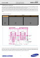
Rev. 1.0 datasheet Unbuffered DIMM DDR3L SDRAM 18. Physical Dimensions 18.1 256Mbx8 based 256Mx72 Module (1 Rank) - M391B5773DH0 Units : Millimeters 9.50 128.95 2.30 17.30 SPD 30.00 ± 0.15 (4X)3.00 ± 0.1 133.35 ± 0.15 (2) 2.50 54.675 A B 47.00 Max 4.0 71.00 2.50 ± 0.20 1.270 ± 0.10 5.00 0.80 ± 0.05 3.80 0.2 ± 0.15 1.50±0.10 1.00 2.50 Detail A Detail B The used device is 256M x8 DDR3L SDRAM, FBGA. DDR3 SDRAM Part NO : K4B2G0846D-HY∗∗ * NOTE : Tolerances on all dimensions ±0.
Rev. 1.0 datasheet Unbuffered DIMM DDR3L SDRAM 18.2 256Mbx8 based 512Mx72 Module (2 Ranks) - M391B5273DH0 Units : Millimeters 9.50 128.95 2.30 17.30 SPD 30.00 ± 0.15 (4X)3.00 ± 0.1 133.35 ± 0.15 (2) 2.50 54.675 A B 47.00 Max 4.0 71.00 2.50 ± 0.20 1.270 ± 0.10 5.00 0.80 ± 0.05 3.80 0.2 ± 0.15 1.50±0.10 1.00 2.50 Detail A Detail B The used device is 256M x8 DDR3L SDRAM, FBGA. DDR3 SDRAM Part NO : K4B2G0846D-HY∗∗ * NOTE : Tolerances on all dimensions ±0.