
User's Manual


page 10/64
Note d’étude / Technical document : URD1– OTL
5665.3
– 003 / 72238 Edition 01
Document Sagemcom Reproduction et divulgation interdites
Sagemcom document. Reproduction and disclosure prohibited
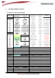
E45
/SIM_RST SIM
/SIM_RST SIM P2P Compliant
E46
/SIM_DATA SIM
/SIM_DATA SIM P2P Compliant
E47
VSIM SIM
VSIM SIM P2P Compliant
E48
VBATT POWER
VBATT POWER P2P Compliant
E49
GND POWER
GND POWER P2P Compliant
E50
/HSET_OUT_P AUDIO
/HSET_OUT_P AUDIO P2P Compliant
E51
/HSET_OUT_N AUDIO
/HSET_OUT_N AUDIO P2P Compliant
As seen in the table above, the two modules are almost pad to pad (P2P) compliant for the main important signals, however
the new HiLoNC V2 M2M module introduce some new interesting features as the digital audio on the PCM bus and the RF
bust indicator signal.
3.2 EASY MIGRATION FROM HILONC (V1) TO HILONC V2
3.2.1 Migration without the use of new features
When upgrading from the HiLoNC V1 to the HiLoNC V2, the SPI bus formerly used was supposed to be left as test points
on your design, then simply left the design as it is, therefore the new PCM bus and RF burst indicator signals will remain
not used.
For the former GPIO4 and GPIO5, if there were both not used, simply add if possible two test points on those signals to be
able to connect a trace cable in case of need. Otherwise, if one or both former GPIO4 and GPIO5 were used, you have to
reallocate those pads to GPIO1, GPIO2 or GPIO3 which remain pad to pad compliant.
3.2.2 Migration with the use of new features
When upgrading from the HiLoNC V1 to the HiLoNC V2, the former SPI bus which was supposed to be left on test points
is now used as the digital audio PCM bus and also the RF indicator signal, simply connect the new signals as described
below in the respective chapter.
The former GPIO4 and GPIO5 signals are now used to connect the UART TXD / RXD trace bus, then add if possible two
test points on those signals to be able to connect a trace cable in case of need.
4. FUNCTIONAL INTEGRATION
The improvement of Silicon technologies heads toward functionality improvement, less power consumption. The
postage stamp sized HiLoNC V2 module meets all these requirement, uses the last high end technology in a
very compact design of only 24 x 24 x 2.6 mm and weighs less than 3 grams.
All digital I/Os among the 51 pads are in 2.8V domain which is suitable for most systems except SIM I/O's
with can also be in the 1.8V domain depending on the used SIM card and POK_IN at 3Vdomain
Analogical I/Os are in the following power domains
• VSIM (the SIM I/Os at 1.8V or 2.9V domain).
• VBACKUP 3V domain
• VGPIO 2.8V domain
• VBAT (from 3.2V to 4.5V domain)
• AUX_ADC0 2.8V domain
• INTMIC_P 2.85V domain
• HSET_OUT_P/N VBAT domain
• ANTENNA (RF power Amplifier is on VBAT domain)
Do not power the module I/O with a voltage over the specified limits, this could damage the module.
Acoustic engineering competences are mandatory to get accurate audio performance on customer’s
product
Radio engineering competences are mandatory to get accurate radio performance on customer’s product.