
Datasheet


3/16
BR25L010-W, BR25L020-W, BR25L040-W, BR25L080-W, BR25L160-W, BR25L320-W, BR25L640-W
Technical Note
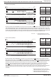
Fig. 2 Pin assignment diagram
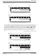
Fig. 4 Input / output timing
SO is output in sync with data fall edge of SCK. Data is output
from the most significant bit MSB.
tCS
tCSH
tSCKH
tPD
tOH
tRO,tFO
tOZ
High-Z
CS
SCK
SI
SO
Fig. 5 HOLD timing
"H"
"L"
tHFS tHFH
tHRS tHRH
tDIS
tHPD
High-Z
tHOZ
Dn+1 Dn-1
n-1
Dn Dn
n+1 n
CS
SCK
SI
SO
HOLD
SCK frequency
SCK high time
Parameter Symbol
–
Min.
–
1. 8 ≤VCC<2.5V
Typ.
2
Max.
200
––
SCK low time 200 ––
CS high time 200 ––
CS setup time
CS hold time
fSCK
tSCKWH
tSCKWL
tCS
tCSS
tCSH
–
Min.
–
2.5≤VCC<5.5V
Typ.
5
Max.
MHz
85
––ns
85
––ns
85
––ns
ns
ns
Unit
200 ––
200 ––
90 ––
SCK setup time
SCK hold time
200 ––
200 ––
SI setup time 40 ––
SI hold time 50 ––
Data output delay time 1
tSCKS
tSCKH
tDIS
tDIH
tPD1
90
––ns
90
––ns
20
––ns
40 ––ns
ns
––150 ––70
Data output delay time 2
(CL2=30pF)
Output hold time
––145
0
––
Output disable time ––250
HOLD setting
setup time
120
––
HOLD setting
hold time
tPD2
tOH
tOZ
tHFS
tHFH
––55 ns
0
––ns
––100 ns
60
––ns
ns
90 ––40 ––
HOLD release
setup time
HOLD release
hold time
120
––
140 ––
Time from HOLD
to output High-Z
––250
Time from HOLD
to output change
––150
SCK
rise time
tHRS
tHRH
tHOZ
tHPD
tRC
60
––ns
70
––ns
––100 ns
––70 ns
μs
––1 ––1
SCK
fall time
OUTPUT
rise time
––1
––100
OUTPUT
fall time
––100
Write time
––5
tFC
tRO
tFO
tE/W
––1 μs
––50 ns
––50 ns
––5ms
85 ––
AC measurement conditions
Load capacity 1
Load capacity 2
Parameter Symbol
–
Min.
–
Limits
Typ.
100
Max.
pF
––30 pF
Input rise time
––50 ns
Input fall time
––50 ns
Input voltage 0.2V
CC/0.8VCC V
Input / output judgment voltage
C
L1
CL2
–
–
–
–
0.3VCC/0.7VCC V
Unit
Pin assignment and description
Operating timing characteristics
(Ta = -40 ~ +85˚C, unless otherwise specified, load capacity CL1 100pF)
CS SO WP GND
SISCKHOLDVCC
Serial data output
Power source to be connected
All input / output reference voltage, 0V
Chip select input
Serial clock input
SI
V
CC
CS
Terminal name
GND
SO
SCK
Input/output
Function
–
–
Input
Input
Output
Hold input
Command communications may be suspended temporarily (HOLD status).
HOLD Input
Write protect input
Write command is prohibited.
Write status register command is prohibited.
WP Input
Input
Start bit, ope code, address, and serial data input
*1NOT 100% TESTED
BR25L010-W
BR25L020-W
BR25L040-W
BR25L080-W
BR25L160-W
BR25L320-W
BR25L640-W
*1
*1
*1
*1
Fig. 3 Input timing
tCS
tDIS
High-Z
tDIH
tRC tFC
tCSS
tSCKS
tSCKWL
tSCKWH
CS
SCK
SI
SO
SI is taken into IC inside in sync with data rise edge of SCK. Input
address and data from the most significant bit MSB.
Sync data input / output timing
*1
*1:BR25L010/020/040-W
2010.07 -
Rev. B
www.rohm.com
© 2010 ROHM Co., Ltd. All rights reserved.