
Datasheet


Technical Note
16/21
BR24T□□□-W Series
www.rohm.com
2011.1 - Rev.H
© 2011 ROHM Co., Ltd. All rights reserved.
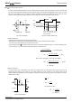
●Cautions on microcontroller connection
○RS
In I
2
C BUS, it is recommended that SDA port is of open drain input/output. However, when to use CMOS input / output of tri state to SDA
port, insert a series resistance Rs between the pull up resistance Rpu and the SDA terminal of EEPROM. This is controls over current
that occurs when PMOS of the microcontroller and NMOS of EEPROM are turned ON simultaneously. Rs also plays the role of
protection of SDA terminal against surge. Therefore, even when SDA port is open drain input/output, Rs can be used.
○Maximum value of Rs
The maximum value of Rs is determined by the following relations.
①SDA rise time to be determined by the capacity (CBUS) of bus line of Rpu and SDA should be tR or below.
And AC timing should be satisfied even when SDA rise time is late.
②The bus electric potential A to be determined by Rpu and Rs the moment when EEPROM outputs 'L' to SDA bus sufficiently secure
the input 'L' level (V
IL
) of microcontroller including recommended noise margin 0.1Vcc.
○Minimum value of Rs
The minimum value of Rs is determined by over current at bus collision. When over current flows, noises in power source line, and
instantaneous power failure of power source may occur. When allowable over current is defined as I, the following relation must be
satisfied. Determine the allowable current in consideration of impedance of power source line in set and so forth. Set the over current to
EEPROM 10mA or below.
RPU
Microcontroller
R
S
EEPROM
Fig.50 I/O circuit diagram Fig.51 Input / output collision timing
ACK
'L' output of EEPROM
'H' output of microcontroller
Over current flows to SDA line by 'H'
output of microcontroller and 'L'
output of EEPROM.
SCL
SDA
Microcontroller
EEPROM
'L'output
R
S
R
PU
'H' output
Over current I
Fig.53 I/O circuit diagram
≦
1.67
[
k
Ω]
≦
0.3×3
-
0.4
-
0.1×3
×
20×10
3
1.1×3
-
0.3×3
R
S
×R
PU
1.1V
CC
-V
IL
Ex.
)
V
CC
=3V
V
IL
=0.3V
CC
V
OL
=0.4V
R
PU
=20k
Ω
∴
R
S
≦
V
IL
-
V
OL
-
0.1V
CC
(V
CC
-
V
OL
)×R
S
+V
OL
+0.1V
CC
≦
V
IL
R
PU
+R
S
V
CC
R
S
V
CC
I
≧
300
[Ω]
∴
Ex.) VCC=3V, I=10mA
R
S
≧
3
10×10
-3
≦
I
R
S
≧