
Manual


16
3595R–DFLASH–11/2012
AT45DB041D
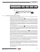
Table 9-5. Program Sector Protection Register Command
Figure 9-3. Program Sector Protection Register
9.1.3 Read Sector Protection Register Command
To read the Sector Protection Register, the
CS pin must first be asserted. Once the CS pin has
been asserted, an opcode of 32H and three dummy bytes must be clocked in via the SI pin. After
the last bit of the opcode and dummy bytes have been clocked in, any additional clock pulses on
the SCK pins will result in data for the content of the Sector Protection Register being output on
the SO pin. The first byte corresponds to sector 0 (0a, 0b), the second byte corresponds to sec-
tor 1 and the last byte (byte 8) corresponds to sector seven. Once the last byte of the Sector
Protection Register has been clocked out, any additional clock pulses will result in undefined
data being output on the SO pin. The
CS must be deasserted to terminate the Read Sector Pro-
tection Register operation and put the output into a high-impedance state.
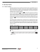
Table 9-6. Read Sector Protection Register Command
Note: xx = Dummy Byte
Figure 9-4. Read Sector Protection Register
9.1.4 Various Aspects About the Sector Protection Register
The Sector Protection Register is subject to a limit of 10,000 erase/program cycles. Users are
encouraged to carefully evaluate the number of times the Sector Protection Register will be
modified during the course of the applications’ life cycle. If the application requires that the Sec-
tor Protection Register be modified more than the specified limit of 10,000 cycles because the
application needs to temporarily unprotect individual sectors (sector protection remains enabled
while the Sector Protection Register is reprogrammed), then the application will need to limit this
practice. Instead, a combination of temporarily unprotecting individual sectors along with dis-
abling sector protection completely will need to be implemented by the application to ensure that
the limit of 10,000 cycles is not exceeded.
Command Byte 1 Byte 2 Byte 3 Byte 4
Program Sector Protection Register 3DH 2AH 7FH FCH
Data Byte
n
Opcode
Byte 1
Opcode
Byte 2
Opcode
Byte 3
Opcode
Byte 4
Data Byte
n + 1
Data Byte
n + 3
CS
Each transition
represents 8 bits
SI
Command Byte 1 Byte 2 Byte 3 Byte 4
Read Sector Protection Register 32H xxH xxH xxH
Opcode X X X
Data Byte
n
Data Byte
n + 1
CS
Data Byte
n + 3
SI
SO
Each transition
represents 8 bits