
Owner's manual


AT27LV020A
9
Rapid
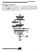
Programming Algorithm
A 100 µs PGM pulse width is used to program. The
address is set to the first location. V
CC
is raised to 6.5V and
V
PP
is raised to 13.0V. Each address is first programmed
with one 100 µs PGM
pulse without verification. Then a
verification/reprogramming loop is executed for each
address. In the event a byte fails to pass verification, up to
10 successive 100 µs pulses are applied with a verification
after each pulse. If the byte fails to verify after 10 pulses
have been applied, the part is considered failed. After the
byte verifies properly, the next address is selected until all
have been checked. V
PP
is then lowered to 5.0V and V
CC
to
5.0V. All bytes are read again and compared with the origi-
nal data to determine if the device passes or fails.