
Manual


AT27C010(L)
3
Note: 1. Minimum voltage is -0.6V dc which may undershoot to -2.0V for pulses of less than 20 ns. Maximum output pin voltage is
V
CC
+ 0.75V dc which may overshoot to +7.0 volts for pulses of less than 20 ns.
Notes: 1. X can be V
IL
or V
IH
.
2. Refer to Programming Characteristics.
3. V
H
= 12.0 ± 0.5V.
4. Two identifier bytes may be selected. All Ai inputs are held low (V
IL
), except A9 which is set to V
H
and A0 which is toggled low
(V
IL
) to select the Manufacturer’s Identification byte and high (V
IH
) to select the Device Code byte.
Absolute Maximum Ratings*
Temperature Under Bias................................ -55°C to +125°C
*NOTICE: Stresses beyond those listed under “Absolute Maxi-
mum Ratings” may cause permanent damage to
the device. This is a stress rating only and func-
tional operation of the device at these or any other
conditions beyond those indicated in the opera-
tional sections of this specification is not implied.
Exposure to absolute maximum rating conditions
for extended periods may affect device reliability.
Storage Temperature ..................................... -65°C to +150°C
Voltage on Any Pin with
Respect to Ground .........................................-2.0V to +7.0V
(1)
Voltage on A9 with
Respect to Ground ......................................-2.0V to +14.0V
(1)
V
PP
Supply Voltage with
Respect to Ground .......................................-2.0V to +14.0V
(1)
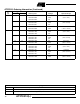
Operating Modes
Mode\Pin CE OE PGM Ai V
PP
Outputs
Read V
IL
V
IL
X
(1)
Ai X D
OUT
Output Disable X V
IH
XXXHigh Z
Standby V
IH
XXXXHigh Z
Rapid Program
(2)
V
IL
V
IH
V
IL
Ai V
PP
D
IN
PGM Verify V
IL
V
IL
V
IH
Ai V
PP
D
OUT
PGM Inhibit V
IH
XX X V
PP
High Z
Product Identification
(4)
V
IL
V
IL
X
A9 = V
H
(3)
A0 = V
IH
or V
IL
A1 - A16 = V
IL
X Identification Code