
Owner's manual


AT27BV4096
5
AC Waveforms for Read Operation
(1)
Notes: 1. Timing measurement references are 0.8V and 2.0V. Input AC drive levels are 0.45V and 2.4V, unless otherwise specified.
2. OE
may be delayed up to t
CE
- t
OE
after the falling edge of CE without impact on t
CE
.
3. OE may be delayed up to t
ACC
- t
OE
after the address is valid without impact on t
ACC
.
4. This parameter is only sampled and is not 100% tested.
5. Output float is defined as the point when data is no longer driven.
6. When reading a 27BV4096, a 0.1
µ
F capacitor is required across V
CC
and ground to suppress spurious voltage transients.
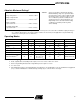
AC Characteristics for Read Operation
V
CC
= 2.7V to 3.6V and 4.5V to 5.5V
Symbol Parameter Condition
AT27BV4096-12 AT27BV4096-15
UnitsMin Max Min Max
t
ACC
(3)
Address to Output Delay
CE
= OE
= V
IL
120 150 ns
t
CE
(2)
CE to Output Delay OE = V
IL
120 150 ns
t
OE
(2)(3)
OE to Output Delay CE = V
IL
35 50 ns
t
DF
(4)(5)
OE or CE High to Output Float,
whichever occurred first
30 40 ns
t
OH
Output Hold from Address, CE or OE,
whichever occurred first
00ns