
Hardware Design V1.0


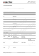
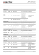


Table Of Contents
- About the Document
- Contents
- Table Index
- Figure Index
- 1 Introduction
- 2 Product Concept
- 3 Application Functions
- 4 Antenna Interface
- 5 Electrical, Reliability and Radio Characteristics
- 6 Mechanical Dimensions
- 7 Storage and Manufacturing
- 8 Appendix A Reference

NB-IoT Module Series
BC95 Hardware Design
BC95_Hardware_Design Confidential / Released 15 / 45
59~66,
71~74,
81~83,
92~94
SWD Interface
Pin Name
Pin No.
I/O
Description
DC Characteristics
Comment
SWD_
DATA
3
IO
Serial wire data signal
V
OL
max=0.4V
V
OH
min=2.4V
V
IL
min=-0.3V
V
IL
max=0.6V
V
IH
min=2.1V
V
IH
max=3.3V
Used for firmware
upgrading.
SWD_
CLK
4
DI
Serial wire clock signal
V
OL
max=0.4V
V
OH
min=2.4V
Reset Interface
Pin Name
Pin No.
I/O
Description
DC Characteristics
Comment
RESET
15
DI
Reset the module
R
PU
≈78kΩ
V
IH
max=3.3V
V
IH
min=2.1V
V
IL
max=0.6V
Pull up internally.
Active low.
Network Status Indicator
Pin Name
Pin No.
I/O
Description
DC Characteristics
Comment
NETLIGHT
18
DO
Network status
indication
V
OL
max=0.4V
V
OH
min=2.4V
If unused, keep this
pin open.
ADC interface
Pin Name
Pin No.
I/O
Description
DC Characteristics
Comment
ADC
21
AI
General purpose analog
to digital converter
Input voltage range:
-0.3V to 4.2V
If unused, keep this
pin open.
UART Port
Pin Name
Pin No.
I/O
Description
DC Characteristics
Comment
RXD
29
DI
Receive data
V
IL
max=0.6V
V
IH
min=2.1V
V
IH
max=3.3V
3.0V power domain.
If unused, keep this
pin open.
TXD
30
DO
Transmit data
V
OL
max=0.4V
V
OH
min=2.4V
3.0V power domain.
If unused, keep this
pin open.
Quectel
Confidential