
Product Info


LTE Standard Module Series
EC25 Series Hardware Design
EC25_Series_Hardware_Design 27 / 134
be designed in schematic and PCB decal, and these pins should be served as a keepout area.
3.3. Pin Description
The following tables show the pin definition of EC25 series module.
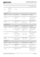
Table 3: I/O Parameters Definition
Table 4: Pin Description
Type
Description
AI
Analog Input
AO
Analog Output
DI
Digital Input
DO
Digital Output
IO
Bidirectional
OD
Open Drain
PI
Power Input
PO
Power Output
Power Supply
Pin Name
Pin No.
I/O
Description
DC Characteristics
Comment
VBAT_BB
59, 60
PI
Power supply for
module’s baseband
part
Vmax = 4.3 V
Vmin = 3.3 V
Vnorm = 3.8 V
It must be provided with
sufficient current up to
0.8 A.
VBAT_RF
57, 58
PI
Power supply for
module’s RF part
Vmax = 4.3 V
Vmin = 3.3 V
Vnorm = 3.8 V
It must be provided with
sufficient current up to
1.8 A in a burst
transmission.
VDD_EXT
7
PO
Provide 1.8 V for
external circuit
Vnorm = 1.8 V
I
O
max = 50 mA
Power supply for
external GPIO’s pull-up