
User Manual


AND9932/D
www.onsemi.com
13
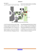
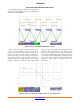
The waveform shown in Figure 16 is a result of driving
two HEMT, GIT, 600 V, 26 A, 56 mW GaNFETs which have
higher current capability compared to the devices used in
Figure 15. To achieve high dV/dt, a significant amount of
drain current, I
D
is required. For example, the measurement
shown is taken at I
D
= 20 A
PK
resulting in a measured V
DS
,
dV/dt = 75 V/ns. The triangular, peak inductor current
appears as DC only because of the time base (2 ns/div)
necessary to make this measurement. The 100 V undershoot
of the VSW waveform is the result of the measurement
technique used to show the high dV/dt and is not actually
present on the switch node.
CONCLUSION
The successful adoption of wide band gap
semiconductors demands a greater awareness of the
negative effects parasitic inductance and capacitance have
in any high voltage, high frequency, PCB design.
A thorough understanding of the importance of electrical
return planes, shielding, current separation, isolation and
careful routing are essential for deriving the maximum
performance benefits offered from GaN technology. This
paper has highlighted the most important PCB design
guidelines that must be adopted for achieving a successful
design using the NCP51820 for driving GaN power switches
used in high−speed power topologies. These techniques
have been validated with measured waveforms and shown
to produce excellent results.
onsemi, , and other names, marks, and brands are registered and/or common law trademarks of Semiconductor Components Industries, LLC dba “onsemi” or its affiliates
and/or subsidiaries in the United States and/or other countries. onsemi owns the rights to a number of patents, trademarks, copyrights, trade secrets, and other intellectual property.
A listing of onsemi’s product/patent coverage may be accessed at
www.onsemi.com/site/pdf/Patent−Marking.pdf. onsemi reserves the right to make changes at any time to any
products or information herein, without notice. The information herein is provided “as−is” and onsemi makes no warranty, representation or guarantee regarding the accuracy of the
information, product features, availability, functionality, or suitability of its products for any particular purpose, nor does onsemi assume any liability arising out of the application or use
of any product or circuit, and specifically disclaims any and all liability, including without limitation special, consequential or incidental damages. Buyer is responsible for its products
and applications using onsemi products, including compliance with all laws, regulations and safety requirements or standards, regardless of any support or applications information
provided by onsemi. “Typical” parameters which may be provided in onsemi data sheets and/or specifications can and do vary in different applications and actual performance may
vary over time. All operating parameters, including “Typicals” must be validated for each customer application by customer’s technical experts. onsemi does not convey any license
under any of its intellectual property rights nor the rights of others. onsemi products are not designed, intended, or authorized for use as a critical component in life support systems
or any FDA Class 3 medical devices or medical devices with a same or similar classification in a foreign jurisdiction or any devices intended for implantation in the human body. Should
Buyer purchase or use onsemi products for any such unintended or unauthorized application, Buyer shall indemnify and hold onsemi and its officers, employees, subsidiaries, affiliates,
and distributors harmless against all claims, costs, damages, and expenses, and reasonable attorney fees arising out of, directly or indirectly, any claim of personal injury or death
associated with such unintended or unauthorized use, even if such claim alleges that onsemi was negligent regarding the design or manufacture of the part. onsemi is an Equal
Opportunity/Affirmative Action Employer. This literature is subject to all applicable copyright laws and is not for resale in any manner.
PUBLICATION ORDERING INFORMATION
TECHNICAL SUPPORT
North American Technical Support:
Voice Mail: 1 800−282−9855 Toll Free USA/Canada
Phone: 011 421 33 790 2910
LITERATURE FULFILLMENT:
Email Requests to: orderlit@onsemi.com
onsemi Website: www.onsemi.com
Europe, Middle East and Africa Technical Support:
Phone: 00421 33 790 2910
For additional information, please contact your local Sales Representative
◊