
Datasheet


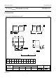


Table Of Contents

2004 Dec 23 3
NXP Semiconductors Product data sheet
15 V low V
CE(sat)
PNP double transistor
PBSS3515VS
LIMITING VALUES
In accordance with the Absolute Maximum Rating System (IEC 60134).
Note
1. Transistor mounted on an FR4 printed-circuit board.
THERMAL CHARACTERISTICS
Notes
1. Transistor mounted on an FR4 printed-circuit board.
2. The only recommended soldering method is reflow soldering.
SYMBOL PARAMETER CONDITIONS MIN. MAX. UNIT
Per transistor unless otherwise specified
V
CBO
collector-base voltage open emitter − −15 V
V
CEO
collector-emitter voltage open base − −15 V
V
EBO
emitter-base voltage open collector − −6 V
I
C
collector current (DC) − −500 mA
I
CM
peak collector current − −1 A
I
BM
peak base current − −100 mA
P
tot
total power dissipation T
amb
≤ 25 °C; note 1 − 200 mW
T
stg
storage temperature −65 +150 °C
T
j
junction temperature − 150 °C
T
amb
operating ambient temperature −65 +150 °C
Per device
P
tot
total power dissipation T
amb
≤ 25 °C; note 1 − 300 mW
SYMBOL PARAMETER CONDITIONS VALUE UNIT
R
th(j-a)
thermal resistance from junction to ambient notes 1 and 2 416 K/W