
Datasheet


MPXA6115A
Sensors
4 Freescale Semiconductor, Inc.
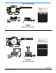
Figure 1 shows a block diagram of the internal circuitry integrated on a pressure sensor chip.
Figure 1. Fully Integrated Pressure Sensor Schematic
On-chip Temperature Compensation and Calibration
Figure 2 illustrates the absolute sensing chip in the basic
Super Small Outline chip carrier (Case 1317).
Figure 3 shows a typical application circuit (output source
current operation).
Figure 4 shows the sensor output signal relative to
pressure input. Typical minimum and maximum output
curves are shown for operation over 0 to 85C temperature
range. The output will saturate outside of the rated pressure
range.
A fluorosilicone gel isolates the die surface and wire bonds
from the environment, while allowing the pressure signal to
be transmitted to the silicon diaphragm. The MPXxx6115A
series pressure sensor operating characteristics, internal
reliability and qualification tests are based on use of dry air as
the pressure media. Media other than dry air may have
adverse effects on sensor performance and long-term
reliability. Contact the factory for information regarding media
compatibility in your application.
Figure 2. Cross Sectional Diagram SSOP/SOP (not to scale)
Figure 3. Typical Application Circuit
(Output Source Current Operation)
Pins 1, 5, 6, 7, and 8 are NO CONNECTS
Sensing
Element
V
OUT
V
S
Gain Stage #2
GND
and Ground
Reference
Shift
Circuitry
Thin Film
Temperature
Compensation
and
Gain Stage #1
3
2
4
Wire Bond
Stainless
Steel Cap
Thermoplastic
Case
Die Bond
Sealed Vacuum Reference
Fluorosilicone
Gel Die Coat
Lead
Frame
Absolute Element
P1
Die
V
S
Pin 2
+5.0 V
GND Pin 3
V
out
Pin 4
MPXxx6115A
to ADC
100 nF
51 K
47 pF