
Datasheet


MX7837/MX7847
Bipolar Operation (4-Quadrant
Multiplication)
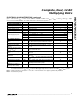
Figure 7 shows the MX7837/MX7847 connected for
binary operation. The offset-binary coding is shown in
Table 4. When V
IN
is an AC signal, the circuit performs
4-quadrant multiplication. R1, R2, and R3 resistors
should be 0.01% ratio matched to maintain gain-error
specifications. On the MX7847, the R
FB
feedback
resistor is internally connected to V
OUT
.
Table 4. Bipolar Code Table
__________Applications Information
Ground Management
The use of an uninterrupted ground plane is strongly
recommended. AC or transient voltages between ana-
log and digital grounds (between AGNDA/AGNDB and
DGND) can inject noise into the analog circuitry.
Connect the MX7837/MX7847 AGNDs and DGND
directly to the ground plane or to a star ground to
ensure that they are at the same potential. In complex
systems with separate analog and digital ground
planes, connect two diodes (1N914 or equivalent) in
inverse parallel between the AGND and DGND pins.
Power-Supply Decoupling
To minimize noise, decouple the V
DD
and V
SS
lines to
DGND using a 10µF capacitor in parallel with a 0.1µF
ceramic capacitor. Minimize capacitor lead lengths for
best noise rejection.
Operation with Reduced
Power-Supply Voltages
The MX7837/MX7847 are specified for operation with
V
DD
/V
SS
= ±11.4V to ±16.5V. However, the output
amplifier requires 2.5V of headroom, so the reference
input should not come within 2.5V of V
DD
/V
SS
in order to
maintain accuracy at full scale.
Complete, Dual, 12-Bit
Multiplying DACs
8 _______________________________________________________________________________________
DAC A
AGNDA V
SS
DGND
R
FBA
*
V
OUTA
*
V
OUT
V
IN
V
DD
V
REFA
V
DD
MX7837
MX7847
* INTERNALLY CONNECTED ON MX7847
V
SS
V
SS
DAC A
AGNDA V
SS
DGND
R
FBA
*
V
OUTA
V
IN
V
DD
V
REFA
MX7837
MX7847
V
OUT
R1
20k
R2
20k
R3
10k
MAX427
V
DD
V
SS
* INTERNALLY CONNECTED
ON MX7847
DAC Latch Contents
MSB LSB
Analog Output, V
OUT
1111 1111 1111
+×
V
2047
2048
IN
1000 0000 0001
+×
V
1
2048
IN
0111 1111 1111
−×
V
1
2048
IN
0000 0000 0000
−×
=−V
2048
2048
V
IN IN
1000 0000 0000 0V
Note : 1LSB
V
2048
IN
=
Figure 6. Unipolar Binary Operation Figure 7. Bipolar Offset Binary Operation