
Datasheet


CS, WR, A0, and A1 control data loading to the input
latches. The eight data inputs accept right-justified
data, which can be loaded to the input latches in any
sequence. If LDAC is held high, loading data to the
input latches will not change the analog output. A0
and A1 determine which input latch will receive the
data when CS and WR are low. Table 2 shows the
control logic truth table.
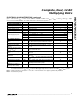
Table 2. MX7837 Truth Table
X = Don't Care
The LDAC input controls 12-bit data transfer from the
input latches to the DAC latches. When LDAC is taken
low, both DAC latches (thus, both analog outputs) are
updated simultaneously. When LDAC is low, the DAC
latches are transparent; DAC data is latched on the ris-
ing edge of LDAC. The LDAC input is asynchronous
and independent of WR. This is useful in many appli-
cations, especially in updating multiple MX7837s simul-
taneously. However, be careful when exercising LDAC
during a write cycle; if an LDAC operation overlaps a
CS and WR operation, invalid data may be latched to
the output. To avoid this, LDAC must remain low after
CS or WR have returned high for a period equal to or
greater than t
8
, the minimum LDAC pulse width.
Unipolar Binary Operation
Figure 6 shows DAC A (MX7837/MX7847) connected
for unipolar binary operation. Similar connections
apply for DAC B. When V
IN
is an AC signal, the circuit
performs 2-quadrant multiplication. Table 3 shows the
code table for this circuit. On the MX7847, the R
FB
feedback resistor is internally connected to V
OUT
.
Table 3. Unipolar Code Table
DAC A
MS
INPUT
LATCH
DAC A LATCH
DAC A
LS
INPUT
LATCH
DAC B
MS
INPUT
LATCH
DAC B
LS
INPUT
LATCH
A1
A0
WR
CS
LDAC
DAC B LATCH
12
12
4
8
4
8
8
DB7 DB0
Figure 4. MX7837 Input Control Logic
DAC Latch Contents
MSB LSB
−×
V
IN
4095
4096
MX7837/MX7847
Complete, Dual, 12-Bit
Multiplying DACs
_______________________________________________________________________________________ 7
Function
1 X 1 No Data Transfer
X 1 1 No Data Transfer
0 0 1 DAC A LS Input Latch Transparent
0 0 1 DAC A MS Input Latch Transparent
0 0 1 DAC B LS Input Latch Transparent
0 0 1 DAC B MS Input Latch Transparent
1 1 0
Updated Simultaneously from
the Respective Input Latches
A0
X
X
0
1
0
1
X
A1
X
X
0
0
1
1
X
ADDRESS VALID
VALID DATA
t
6
t
7
t
1
t
2
t
5
t
3
t
4
A0/A1
CS
WR
DATA
LDAC
t
8
Figure 5. MX7837 Write-Cycle Timing Diagram
Note : 1LSB
V
4096
IN
=
Analog Output, V
OUT
1111 1111 1111
1000 0000 0000
−×
=−V
1
2
V
IN IN
2048
4096
0000 0000 0001
−×
V
IN
1
4096
0000 0000 0000 0V