
Instruction Manual


___________________________________________________________________________________________________________ 9-6
MAXQ7667 User’s Guide
9.1.1.1 SPI Data Buffer Register (SPIB)
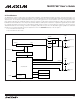
The SPI data buffer register (SPIB) uses the SPI port shift register for write operations and a separate read buffer for read operations.
Bit 15 is the MSB of the register and bit 0 is the LSB of the register. This register is word- or byte-access enabled and the data is shift-
ed towards the MSB only. The port is double buffered on read and single buffered on write. See Figure 9-2. Write access to this regis-
ter is allowed only outside of an active transfer cycle (STBY = 0).
SPIB writes are blocked if the shift register is busy (STBY = 1) and the write collision flag will be set.
This register is accessed through direct read and write addressing and is cleared on all forms of reset (power-on reset, brownout reset,
external reset, watchdog reset, and internal system reset).
Register Description:
SPI Data Buffer Register
Register Name: SPIB
Register Address: Module 01h, Index 06h
Bits 15 to 0: SPIB Data Bits 15:0 (SPIB[15:0])
. The SPIB data port is the register location for the SPI read and write data. Write access
is only allowed when the port has completed a transfer. The read port is double buffered to allow time for firmware to read data into
the µC. SPIB7 is the MSB when 8-bit data transfers are used; SPIB15 is the MSB for 16-bit data.
Bit #
15 14 13 12 11 10 98
Name SPIB15 SPIB14 SPIB13 SPIB12 SPIB11 SPIB10 SPIB9 SPIB8
Reset 0 0 0 0 0 0 0 0
Access rw rw rw rw rw rw rw r w
Bit #
76543210
Name SPIB7 SPIB6 SPIB5 SPIB4 SPIB3 SPIB2 SPIB1 SPIB0
Reset 0 0 0 0 0 0 0 0
Access rw rw rw rw rw rw rw r w
r = read, w = write