
Owner's manual


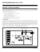


3.1.1 Analog I/O Pins
The analog I/O module has 24 pins associated with the analog functions on the microcontroller. Table 3-1 shows the external interface
signals used by the analog I/O module.
Table 3-1. Analog I/O Module Signals
MAXQ7665/MAXQ7666 User’s Guide
3-6
SIGNAL FUNCTION
AIN15
AIN14
AIN13
AIN12
AIN11
AIN10
AIN9
AIN8
AIN7
AIN6
AIN5
AIN4
AIN3
AIN1
ADC Analog Input #. These are dedicated analog input pins connected through the internal analog multiplexer to the PGA and ADC.
The analog multiplexer supports 8 differential-input measurements. In differential-input mode, the inputs are paired: AIN14 to
AIN15, AIN12 to AIN13, AIN10 to AIN11, AIN8 to AIN9, AIN6 to AIN7, AIN4 to AIN5, AIN2 to AIN3, AIN0 to AIN1.
AIN2/TS2
AIN0/TS0
ADC Analog Input/Remote Temperature Sensor. Analog input pins AIN2 and AIN0 are shared with the remote temperature-sensor
drive line. If the remote temperature-sensor drive circuit is not selected, the pin can be used as a differential input to the
multiplexer. In differential-input configuration, AIN2 is referenced to AIN3 while AIN0 is referenced to AIN1. When selected, the
remote temperature-sensor drive circuit supplies suitable current to drive an external diode-connected transistor to monitor
temperature away from the microcontroller. The remote temperature measurement can be made either in single-ended or
differential configuration. Note: In differential configuration, AIN3 is used as the return path for AIN2 and AIN1 is used as the return
path for AIN0.
DACOUT
DAC Voltage Output. DACOUT is a dedicated output pin. If the DAC is disabled, the pin is configured as a 100k pulldown
resistor to AGND. The DACOUT line can be used for precision drive applications.
P0.4/ADCCNV
ADC Conversion Start Input/Port 0 Data Bit 4. The ADC conversion start is a shared pin with the general-purpose digital I/O port 0
bit 4. As ADCCNV, this pin can trigger ADC sampling and conversion on a rising or falling edge. After power-up or a reset this
pin defaults to a digital I/O port pin with pullup enabled.
P0.5/DACLOAD
DAC Load Input/Port 0 Data Bit 5. The DAC load is a shared pin with the general-purpose digital I/O port 0 bit 5. As DACLOAD,
this pin can trigger DAC conversion by loading the DAC output register on a rising or falling edge. After power-up or a reset this
pin defaults to a digital I/O port pin with pullup enabled.
REFADC
ADC Reference Input. The REFADC input pin is used to supply an external precision voltage reference to the ADC. The REFADC
can handle a voltage range from 1V to AVDD. The REFADC input determines the full-scale range (FSR) of the internal 12-bit ADC.
REFDAC
DAC Reference Input. The REFDAC input pin is used to supply an external precision voltage reference to the DAC. The REFDAC
can handle a voltage range from 0 to AVDD. The REFDAC input determine the full-scale range (FSR) of the internal 12-bit DAC.
AVDD
Analog V
DD
Supply. The analog supply voltage is +5.0V for the MAXQ7665/MAXQ7666.
AGND Analog Ground (2 pins)
EP
Exposed Paddle. The MAXQ7665/MAXQ7666 TQFN package has an exposed paddle on the bottom of the package, providing a
very low thermal resistance path for heat removal from the IC, as well as low-inductance path to ground. The pad is electrically
connected to AGND and should be soldered to the circuit board analog ground plane for proper thermal and electrical
performance. Refer to Maxim’s Application Note HFAN-08.1: Thermal Considerations for QFN and Other Exposed Pad Packages
for additional information.
Maxim Integrated