
Owner's manual


MAXQ7665/MAXQ7666 User’s Guide
4-65
The CAN 0 bus timing register 0 (C0BT0) contains the control bits for the PHASE_SEG1 and PHASE_SEG2 time segments as well as
the baud-rate prescaler (BPR5:BPR0) bits. CAN 0 bus timing register 1 (C0BT1) controls the sampling rate, the time segment two bits
that control the number of clock cycles assigned to the phase segment 2 portion, and the time segment one bits that determine the
number of clock cycles assigned to the phase segment 1 portion. The value of both of the bus timing registers is automatically loaded
into the CAN module following each software change of the SWINT bit from a 1 to a 0 by the microcontroller. The bit timing parame-
ters must be configured before starting operation of the CAN module. These registers can only be modified during a software initial-
ization (SWINT = 1), when the CAN module is NOT in a BUSOFF mode, and after the removal of a system reset or a CAN reset. To
avoid unpredictable behavior of the CAN module, the bus timing registers should never be written with all zeros. To prevent this, the
SWINT is forced to 0 when TSEG1 = TSEG2 = 00h.
The timing of the various time segments is determined by the following formulas. Most users never need to perform these calculations,
as other devices already attached to the network dictate the bus timing parameters.
where BRPV is the CAN baud-rate prescaler value found in the earlier description of the C0BT0 and COR registers, f
OSC
is the crys-
tal or external oscillator frequency of the microprocessor, and TS1_LEN and TS2_LEN are listed in the description of the
TSEG26:TSEG24 and TSEG13:TSEG10 bits in the CAN bus timing register 1 (C0BT1). SJW is listed in the description of the SJW1:SJW0
bits in the CAN bus timing register 0 (C0BT0). The CAN clock divide (CCD) value is a factor tied to the current microcontroller system
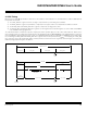
clock selection CKCN (see the peripheral register description) and can be referenced in the following table.
Table 4-4. CAN Clock Divide Selection
t
BRPV CCD
f
tt
t TS LEN t
t TS LEN t
t SJW t
t per bit
baud rate t
Only eger values are permitted
QU
OSC
SYNC SEG QU
TSEG QU
TSEG QU
SJW QU
QU
QU
=
×
=×
=
()
×
=
()
×
=
()
×
=
×
_
_
_
( int .)
1
1
1
1
1
2
CD1 CD0 PMME CCD
0001
0102
1004
1108
001256
011256
101256
1 1 1 Reserved
Maxim Integrated