
Users Guide: MAXQ2010 Supplement User Manual


MAXQ Family User’s Guide:
MAXQ2010 Supplement
21-8
21.2.4 Timer B Clock Output Mode
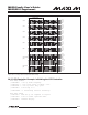
Timer B can be configured to drive a clock output on the TBA pin as shown in Figure 21-4. For the timer to operate in
this mode, the capture/reload select bit (CP/RLB = TBnCN.0) and the counter/timer select bit (C/TB = TBnCN.15) must
be cleared to 0, and the Timer B output-enable bit (TBOE = TBnCN.5) ) must be set to 1. In this mode, the DCEN bit
has no effect. The clock signal output is a 50% duty-cycle square wave with a frequency given by the equation:
Clock Output Frequency = System Clock/(2 x TBnR)
Therefore, for a system clock of 1MHz and a TBnR register value of 0005h (arbitrary example), the clock output fre-
quency is 100kHz.
21.2.5 Timer B PWM/Output Control Functionality
The PWM/output control function is enabled whenever either of the TCBS or TBCR bits (TBnCN[12:11]) is set to 1. Table
21-4 shows how these bits determine the specific operation.
Figure 21-4. Timer B Clock Output Mode Block Diagram
Table 21-4. Timer B PWM/Output Control Function
15
0
TBnR
TBnV
0000h
SYSTEM
CLOCK
TBA PIN
TBA PIN
TRB = TBnCN.2
/CLK
C/TB = TBnCN.15 = 0
DIVIDE BY 2
FALLING
EDGE
TBB PIN
TIMER INTERRUPT
EXENB = TBnCN.3
COMPARE
0 15
EXFB = TBnCN.6
TBPS[2:0] = TBnCN[10:8]
2
(2 x TBPS[2:0])
TBCS:TBCR FUNCTION INITIAL STATE (IF TRB = 0)
00 None (Disabled) No change
01 Reset on TBnC Match, Set on 0000h Low
10 Set on TBnC Match, Reset on TBnR Match High
11 Toggle on TBnC Match No change