
Datasheet


MAX9945
For voltage-output sensors, a noninverting amplifier is
typically used to buffer and/or apply a small gain to, the
input voltage signal. Due to the extremely high imped-
ance of the sensor output, a low input bias current with
a small temperature variation is very important for these
applications.
Power-Supply Decoupling
The MAX9945 operates from a +4.75V to +38V, V
EE
ref-
erenced power supply. Bypass the power-supply
inputs V
CC
and V
EE
to a quiet copper ground plane,
with a 0.1µF ceramic capacitor in parallel with a 4.7µF
electrolytic capacitor, placed close to the leads.
Layout Techniques
A good layout is critical to obtaining high performance
especially when interfacing with high-impedance sen-
sors. Use shielding techniques to guard against para-
sitic leakage paths. For transimpedance applications,
for example, surround the inverting input, and the
traces connecting to it, with a buffered version of its
own voltage. A convenient source of this voltage is the
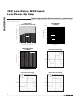
noninverting input pin. Pins 1, 5, and 8 on the µMAX
package are unconnected, and can be connected to
an analog common potential, or to the driven guard
potential, to reduce leakage on the inverting input.
A good layout guard rail isolates sensitive nodes, such
as the inverting input of the MAX9945 and the traces
connecting to it (see Figure 1), from varying or large volt-
age differentials that otherwise occur in the rest of the
circuit board. This reduces leakage and noise effects,
allowing sensitive measurements to be made accurately.
Take care to also decrease the amount of stray capaci-
tance at the op amp’s inputs to improve stability. To
achieve this, minimize trace lengths and resistor leads
by placing external components as close as possible to
the package. If the sensor is inherently capacitive, or is
connected to the amplifier through a long cable, use a
low-value feedback capacitor to control high-frequency
gain and peaking to stabilize the feedback loop.
38V, Low-Noise, MOS-Input,
Low-Power Op Amp
8 _______________________________________________________________________________________
1
2
8
7
μMAX
3
4
6
5
MAX9945
IN-
IN+
MAX9945
V
OUT
+
-
+
Figure 1. Shielding the Inverting Input to Reduce Leakage
MAX9945
IN+
IN-
10kΩ
10kΩ
Figure 2. Input Differential Voltage Protection