
Datasheet


10 _____________________________________________________________________________________
MAX98306
Stereo 3.7W Class D Amplifier
Applications Information
Filterless Class D Operation
Traditional Class D amplifiers require an output filter.
The filter adds cost and size and decreases THD perfor-
mance. The IC’s filterless modulation scheme does not
require an output filter.
Because the switching frequency of the IC is well
beyond the bandwidth of most speakers, voice coil
movement due to the switching frequency is very small.
Use a speaker with a series inductance > 10FH. Typical
8I speakers exhibit series inductances in the 20FH to
100FH range.
Component Selection
Power-Supply Input (PVDD)
PVDD powers the speaker amplifier. PVDD ranges from
2.6V to 5.5V. Bypass PVDD with 0.1FF and 10FF capaci-
tors to PGND. Apply additional bulk capacitance at the
device if long input traces between PVDD and the power
source are used.
Input Filtering
The input-coupling capacitor (C
IN
), in conjunction with
the amplifier’s internal input resistance (R
IN
), forms a
highpass filter that removes the DC bias from the incom-
ing signal. These capacitors allow the amplifier to bias
the signal to an optimum DC level.
Assuming zero source impedance, C
IN
is:
−
=
π ×
IN
3dB IN
1
C
2 f R
where f
-3dB
is the -3dB corner frequency and R
IN
is the
typical value as specified in the Electrical Characteristics
table. Use capacitors with adequately low-voltage coeffi-
cients for best low-frequency THD performance. Table 2
shows calculated capacitance values based on a 20Hz
highpass filter.
Layout and Grounding
Proper layout and grounding are essential for optimum
performance. Good grounding improves audio perfor-
mance and prevents switching noise from coupling into
the audio signal.
Use wide, low-resistance output traces. As the load
impedance decreases, the current drawn from the
device increases. At higher current, the resistance of the
output traces decrease the power delivered to the load.
For example, if 2W is delivered from the device output to
a 4I load through 100mI of total speaker trace, 1.904W
is delivered to the speaker. If power is delivered through
10mI of total speaker trace, 1.99W is delivered to the
speaker. Wide output, supply, and ground traces also
improve the power dissipation of the device.
The IC is inherently designed for excellent RF immunity.
For best performance, add ground fills around all signal
traces on top or bottom PCB planes.
Chip Information
PROCESS: CMOS
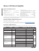
Table 2. Capacitance Value for 20Hz
Highpass Filter
GAIN
R
IN
(kI)
C
IN
for 20Hz (nF)
18 33 241
15 46 173
12 65 122
9 93 86
6 131 61