
Datasheet


MAX9724C/MAX9724D
Detailed Description
The MAX9724C/MAX9724D stereo headphone ampli-
fiers feature Maxim’s DirectDrive architecture, eliminat-
ing the large output-coupling capacitors required by
conventional single-supply headphone amplifiers. The
device consists of two 60mW Class AB headphone
amplifiers, undervoltage lockout (UVLO)/shutdown con-
trol, charge pump, and comprehensive click-and-pop
suppression circuitry (see the
Functional
Diagram/Typical Operating Circuits
). The charge pump
inverts the positive supply (V
DD
), creating a negative
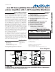
supply (PVSS). The headphone amplifiers operate from
these bipolar supplies with their outputs biased about
PGND (Figure 1). The benefit of this PGND bias is that
the amplifier outputs do not have a DC component. The
large DC-blocking capacitors required with convention-
al headphone amplifiers are unnecessary, conserving
board space, reducing system cost, and improving fre-
quency response. The MAX9724C/MAX9724D feature
an undervoltage lockout that prevents operation from
an insufficient power supply and click-and-pop sup-
pression that eliminates audible transients on startup
and shutdown. The MAX9724C/MAX9724D also feature
thermal-overload and short-circuit protection.
DirectDrive
Conventional single-supply headphone amplifiers have
their outputs biased about a nominal DC voltage (typi-
cally half the supply) for maximum dynamic range.
Large-coupling capacitors are needed to block this DC
bias from the headphone. Without these capacitors, a
significant amount of DC current flows to the head-
phone, resulting in unnecessary power dissipation and
possible damage to both headphone and headphone
amplifier.
Maxim’s DirectDrive architecture uses a charge pump
to create an internal negative supply voltage, allowing
the MAX9724C/MAX9724D outputs to be biased about
GND. With no DC component, there is no need for the
large DC-blocking capacitors. The MAX9724C/
MAX9724D charge pumps require two small ceramic
capacitors, conserving board space, reducing cost,
and improving the frequency response of the head-
phone amplifier. See the Output Power vs. Load
Resistance and Charge-Pump Capacitor Size graph in
the
Typical Operating Characteristics
for details of the
possible capacitor sizes. There is a low DC voltage on
the amplifier outputs due to amplifier offset. However,
the offsets of the MAX9724C/MAX9724D are typically
1.5mV, which, when combined with a 32Ω load, results
in less than 47µA of DC current flow to the head-
phones.
Charge Pump
The MAX9724C/MAX9724D feature a low-noise charge
pump. The 270kHz switching frequency is well beyond
the audio range and does not interfere with audio sig-
nals. The switch drivers feature a controlled switching
speed that minimizes noise generated by turn-on and
turn-off transients. The di/dt noise caused by the para-
sitic bond wire and trace inductance is minimized by
limiting the switching speed of the charge pump.
Although not typically required, additional high-fre-
quency noise attenuation can be achieved by increas-
ing the value of C2 (see the
Functional Diagram/Typical
Operating Circuits
).
RF Susceptibility
Modern audio systems are often subject to RF radiation
from sources like wireless networks and cellular phone
networks. Although the RF radiation is out of the audio
band, many signals, in particular GSM signals, contain
bursts or modulation at audible frequencies. Most ana-
log amplifiers demodulate the low-frequency envelope,
adding noise to the audio signal. The architecture of
Low RF Susceptibility DirectDrive Stereo Head-
phone Amplifier with 1.8V Compatible Shutdown
_______________________________________________________________________________________ 9
V
DD
-V
DD
GND
V
OUT
CONVENTIONAL DRIVER-BIASING SCHEME
DirectDrive BIASING SCHEME
V
DD
/2
V
DD
V
DD
GND
V
OUT
2V
DD
Figure 1. Conventional Driver Output Waveform vs.
MAX9724C/MAX9724D Output Waveform