
Datasheet


MAX9174/MAX9175
670MHz LVDS-to-LVDS and Anything-to-LVDS
1:2 Splitters
4 _______________________________________________________________________________________
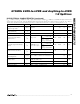
AC ELECTRICAL CHARACTERISTICS
(V
CC
= +3.0V to +3.6V, R
L
= 100Ω±1%, C
L
= 5pF, differential input voltage |V
ID
| = 0.15V to 1.2V, MAX9174 input common-mode volt-
age, V
CM
= |V
ID
/2| to (2.4V - |V
ID
/2|), MAX9175 input common-mode voltage V
CM
= |V
ID
/2| to (V
CC
- |V
ID
/2|), PD_ = high, T
A
= -40°C
to +85°C, unless otherwise noted. Typical values are at V
CC
= +3.3V, |V
ID
| = 0.2V, V
CM
= +1.25V, T
A
= +25°C.) (Notes 5, 6, 7)
PARAMETER
SYMBOL
CONDITIONS
MIN TYP MAX
UNITS
High-to-Low Propagation Delay t
PHL
Figures 4, 5
1.33 2.38 3.23
ns
Low-to-High Propagation Delay t
PLH
Figures 4, 5
1.33 2.39 3.23
ns
Added Deterministic Jitter t
DJ
Figures 4, 5 (Note 8) 80
ps
(P-P)
Added Random Jitter t
RJ
Figures 4, 5 1.0
ps
(RMS)
Pulse Skew t
PLH
- t
PHL
t
SKP
Figures 4, 5 10
141
ps
Output-to-Output Skew t
SKOO
Figure 6 14 45 ps
t
SKPP1
Figures 4, 5 (Note 9) 0.4 1.3
Part-to-Part Skew
t
SKPP2
Figures 4, 5 (Note 10) 1.9
ns
Rise Time t
R
Figures 4, 5
110 257 365
ps
Fall Time t
F
Figures 4, 5
110 252 365
ps
Power-Down Time t
PD
Figures 7, 8 10 13 ns
PD0, PD1 = L → H, Figures 7, 8
18 35 µs
PD0 = H, PD1 = L → H, Figures 7, 8 92
103
Power-Up Time t
PU
PD1 = H, PD0 L → H, Figures 7, 8 92
103
ns
Maximum Data Rate D
RMAX
Figures 4, 5, V
OD
≥ 250mV
(Note 11)
800
Mbps
Maximum Switching Frequency f
MAX
Figures 4, 5, V
OD
≥ 250mV (Note 11)
670
MHz
f
IN
= 670MHz 55 65
Switching Supply Current I
CCSW
f
IN
= 155MHz 35 44
mA
PRBS Supply Current I
CCPR
D
R
= 800Mbps, 2
23
- 1 PRBS input 37 46 mA
Note 1: Current into a pin is defined as positive. Current out of a pin is defined as negative. All voltages are referenced to ground
except V
TH
, V
TL
, V
ID
, V
OD
, and ∆V
OD
.
Note 2: Maximum and minimum limits over temperature are guaranteed by design and characterization. Devices are 100% tested at
T
A
= +25°C.
Note 3: Tolerance on all external resistors (including figures) is ±1%.
Note 4: Guaranteed by design.
Note 5: AC parameters are guaranteed by design and characterization and are not production tested. Limits are set at ±6 sigma.
Note 6: C
L
includes scope probe and test jig capacitance.
Note 7: Pulse-generator output for differential inputs IN+, IN- (unless otherwise noted): f = 670MHz, 50% duty cycle, R
O
= 50Ω, t
R
=
700ps, and t
F
= 700ps (0% to 100%). Pulse-generator output for single-ended inputs PD0, PD1: t
R
= t
F
= 1.5ns (0.2V
CC
to
0.8V
CC
), 50% duty cycle, V
OH
= V
CC
+ 1.0V settling to V
CC
, V
OL
= -1.0V settling to zero, f = 10kHz.
Note 8: Pulse-generator output for t
DJ
: |V
OD
| = 0.15V, V
OS
= 1.25V, data rate 800Mbps, 2
23
- 1 PRBS, R
O
= 50Ω, t
R
= 700ps, and t
F
= 700ps (0% to 100%).
Note 9: t
SKPP1
is the magnitude of the difference of any differential propagation delays between devices operating under identical
conditions.
Note 10: t
SKPP2
is the magnitude of the difference of any differential propagation delays between devices operating over rated con-
ditions.
Note 11: Meets all AC specifications.