
Datasheet


MAX9111/MAX9113
Single/Dual LVDS Line Receivers with
Ultra-Low Pulse Skew in SOT23
_______________________________________________________________________________________ 7
_______________Detailed Description
LVDS Inputs
The MAX9111/MAX9113 feature LVDS inputs for inter-
facing high-speed digital circuitry. The LVDS interface
standard is a signaling method intended for point-to-
point communication over a controlled impedance
media, as defined by the ANSI/EIA/TIA-644 standards.
The technology uses low-voltage signals to achieve fast
transition times, minimize power dissipation, and noise
immunity. Receivers such as the MAX9111/MAX9113
convert LVDS signals to CMOS/LVTTL signals at rates
in excess of 500Mbps. The devices are capable of
detecting differential signals as low as 100mV and as
high as 1V within a 0V to 2.4V input voltage range . The
LVDS standard specifies an input voltage range of 0 to
2.4V referenced to ground.
Fail-Safe
The fail-safe feature sets the output to a high state
when the inputs are undriven and open, terminated, or
shorted. When using one channel in the MAX9113,
leave the unused channel open. The fail-safe feature is
not guaranteed to be operational above +85°C.
ESD Protection
As with all Maxim devices, ESD-protection structures are
incorporated on all pins to protect against electrostatic
discharges encountered during handling and assembly.
The receiver inputs of the MAX9111/MAX9113 have extra
protection against static electricity. Maxim’s engineers
have developed state-of-the-art structures to protect
these pins against ESD of ±11kV without damage. The
ESD structures withstand high ESD in all states: normal
operation, shutdown, and powered down.
ESD protection can be tested in various ways; the
receiver inputs of this product family are characterized
for protection to the limit of ±11kV using the Human
Body Model.
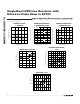
Human Body Model
Figure 3a shows the Human Body Model, and Figure
3b shows the current waveform it generates when dis-
charged into a low impedance. This model consists of a
100pF capacitor charged to the ESD voltage of interest,
which is then discharged into the test device through a
1.5kΩ resistor.
Pin Description
PIN
MAX9111 MAX9113
SOT23-8 SO-8 SOT23-8 SO-8
NAME FUNCTION
1818V
CC
Power Supply
2525GNDGround
8181IN-/IN1- Receiver Inverting Differential Input
7272IN+/IN1+ Receiver Noninverting Differential Input
— — 5 4 IN2- Receiver Inverting Differential Input
— — 6 3 IN2+ Receiver Noninverting Differential Input
3737OUT/OUT1 Receiver Output
— — 4 6 OUT2 Receiver Output
4, 5, 6 3, 4, 6 — — N.C. No Connection. Not internally connected.