
Datasheet


MAX8702/MAX8703
Dual-Phase MOSFET Drivers
with Temperature Sensor
______________________________________________________________________________________ 11
the current limit and cause the fault latch to trip. The
MOSFETs must have a good-sized heatsink to handle
the overload power dissipation. The heat sink can be a
large copper field on the PC board or an externally
mounted device.
The Schottky diode only conducts during the dead time
when both the high-side and low-side MOSFETs are off.
Choose a Schottky diode with a forward voltage low
enough to prevent the low-side MOSFET body diode
from turning on during the dead time, and a peak cur-
rent rating higher than the peak inductor current. The
Schottky diode must be rated to handle the average
power dissipation per switching cycle. This diode is
optional and can be removed if efficiency is not critical.
IC Power Dissipation and
Thermal Considerations
Power dissipation in the IC package comes mainly from
driving the MOSFETs. Therefore, it is a function of both
switching frequency and the total gate charge of the
selected MOSFETs. The total power dissipation when
both drivers are switching is given by:
PD(IC) = I
BIAS
x 5V
where I
BIAS
is the bias current of the 5V supply calcu-
lated in the 5V Bias Supply (V
DD
and V
CC
) section .
The rise in die temperature due to self-heating is given
by the following formula:
∆T
J
= PD(IC) x θ
JA
where PD(IC) is the power dissipated by the device, and
θ
JA
is the package’s thermal resistance. The typical ther-
mal resistance is 59.3°C/W for the 4mm x 4mm thin QFN
package. For example, if the MAX8702 dissipates
500mW of power within the IC, this corresponds to a 30°C
shift in the die temperature in the thin QFN package.
PC Board Layout Considerations
The MAX8702/MAX8703 MOSFET drivers source and
sink large currents to drive MOSFETs at high switching
speeds. The high di/dt can cause unacceptable ringing
if the trace lengths and impedances are not well con-
trolled. The following PC board layout guidelines are
recommended when designing with the device:
1) Place V
CC
and V
DD
decoupling capacitors as close
to their respective pins as possible.
2) Minimize the high-current loops from the input capaci-
tor, upper-switching MOSFET, and low-side MOSFET
back to the input capacitor negative terminal.
3) Provide enough copper area at and around the
switching MOSFETs and inductors to aid in thermal
dissipation.
4) Connect the PGND1 and PGND2 pins as close as
possible to the source of the low-side MOSFETs.
5) Keep LX traces away from sensitive analog compo-
nents and nodes. Place the IC and analog compo-
nents on the opposite side of the board from the
power-switching node if possible.
6) Use two or more vias for DL and DH traces when
changing layers to reduce via inductance.
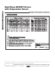
Figure 5 shows a PC board layout example.
POWER
GROUND
OUTPUT
CONNECT AGND AND
PGND_ BENEATH THE
CONTROLLER AT ONE
POINT ONLY AS SHOWN
VIA TO POWER
GROUND
C
IN
C
IN
INDUCTOR
INPUT
USE DOUBLE
VIAS FOR DL_
C
IN
INDUCTOR
C
IN
C
OUT
C
OUT
C
OUT
C
OUT
Figure 5. PC Board Layout Example