
Datasheet


MAX860/MAX861
50mA, Frequency-Selectable,
Switched-Capacitor Voltage Converters
8
Maxim Integrated
MAX860
MAX861
“n”
MAX860
MAX861
“1”
8
7
5
V
OUT
C2
8
7
+V
IN
C1C1
22
33
445
V
OUT
= -V
IN
R
OUT
=
R
OUT
OF SINGLE DEVICE
NUMBER OF DEVICES
…
…
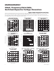
Figure 2. Paralleling MAX860s or MAX861s to Reduce Output
Resistance
MAX860
MAX861
“n”
MAX860
MAX861
“1”
8
7
5
V
OUT
C2
8
7
+V
IN
C1
C2
C1
22
33
445
V
OUT
= -nV
IN
…
…
Figure 1. Cascading MAX860s or MAX861s to Increase
Output Voltage
Flying Capacitor, C1
Increasing the size of the flying capacitor reduces the
output resistance.
Output Capacitor, C2
Increasing the size of the output capacitor reduces the
output ripple voltage. Decreasing its ESR reduces both
output resistance and ripple. Smaller capacitance val-
ues can be used if one of the higher switching frequen-
cies is selected, if less than the maximum rated output
current (50mA) is required, or if higher ripple can be
tolerated. The following equation for peak-to-peak rip-
ple applies to both the inverter and doubler circuits.
I
OUT
V
RIPPLE
= ———————— + 2 x I
OUT
x ESR
C2
2 x f
S
x C2
Bypass Capacitor
Bypass the incoming supply to reduce its AC impedance
and the impact of the MAX860/MAX861’s switching
noise. The recommended bypassing depends on the cir-
cuit configuration and where the load is connected.
When the inverter is loaded from OUT to GND or the
doubler is loaded from V
DD
to GND, current from the
supply switches between 2 x I
OUT
and zero. Therefore,
use a large bypass capacitor (e.g., equal to the value
of C1) if the supply has a high AC impedance.
When the inverter and doubler are loaded from V
DD
to
OUT, the circuit draws 2 x I
OUT
constantly, except for
short switching spikes. A 0.1µF bypass capacitor is
sufficient.
Cascading Devices
Two devices can be cascaded to produce an even
larger negative voltage, as shown in Figure 1. The
unloaded output voltage is nominally -2 x V
IN
, but this is
reduced slightly by the output resistance of the first
device multiplied by the quiescent current of the sec-
ond. The output resistance of the complete circuit is
approximately
five times
the output resistance of a sin-
gle MAX860/MAX861.
Three or more devices can be cascaded in this way,
but output resistance rises dramatically, and a better
solution is offered by inductive switching regulators
(such as the MAX755, MAX759, MAX764, or MAX774).
Connect LV as with a standard inverter circuit (see
Pin
Description
).
The maximum load current and startup current of nth
cascaded circuit must not exceed the maximum output
current capability of (n-1)th circuit to ensure proper
startup.
Paralleling Devices
Paralleling multiple MAX860s or MAX861s reduces the
output resistance. As illustrated in Figure 2, each
device requires its own pump capacitor (C1), but the
reservoir capacitor (C2) serves all devices. C2’s value
should be increased by a factor of n, where n is the
number of devices. Figure 2 shows the equation for cal-
culating output resistance. An alternative solution is to
use the MAX660 or MAX665, which are capable of sup-
plying up to 100mA of load current. Connect LV as with
a standard inverter circuit (see
Pin Description
).
Combined Doubler/Inverter
In the circuit of Figure 3, capacitors C1 and C2 form the
inverter, while C3 and C4 form the doubler. C1 and C3
are the pump capacitors; C2 and C4 are the reservoir
capacitors. Because both the inverter and doubler use
part of the charge-pump circuit, loading either output
causes both outputs to decline towards GND. Make